This appendix contains information about the connector pinouts, which are the same for Sun Fire X4100/X4100 M2 and X4200/X4200 M2 servers.
| Note - The information in this appendix applies to all Sun Fire X4100/X4100 M2 and X4200/X4200 M2 servers, unless otherwise noted in the text.
|
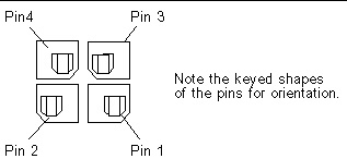
E.1 USB Connector
The USB connector pins and their corresponding descriptions are shown in the figure and table in this section.
FIGURE E-1 USB Connector

TABLE E-1 USB Connector Pinouts
|
Pin Number
|
Pin Name
|
Description
|
|
1
|
+5V
|
+5V supply
|
|
2
|
Data-
|
Negative side of differential for data
|
|
3
|
Data+
|
Positive side of differential for data
|
|
4
|
Gnd
|
Ground
|
| Note - The maximum output supply current for each USB port on the server is 500mA.
|
E.2 Serial Connector
The RJ-45 Serial connector pins and their corresponding descriptions are shown in the figure and table in this section.
FIGURE E-2 Serial Connector

TABLE E-2 Serial Connector Pinouts
|
Pin Number
|
Pin Name
|
Description
|
|
1
|
RTS
|
Ready to send
|
|
2
|
DTR
|
Data terminal ready
|
|
3
|
TXD
|
Transmit data
|
|
4
|
GND
|
Ground
|
|
5
|
GND
|
Ground
|
|
6
|
RXD
|
Receive data
|
|
7
|
DSR
|
Data send ready
|
|
8
|
CTS
|
Clear to send
|
E.3 10/100BASE-T Connector
The RJ-45 10/100BASE-T (Net Management) connector pins and their corresponding descriptions are shown in the figure and in this section.
FIGURE E-3 10/100BASE-T Connector

TABLE E-3 10/100BASE-T Connector Pinouts
|
Pin Number
|
Pin Name
|
Description
|
|
1
|
TX+
|
Positive side of transmit data
|
|
2
|
TX-
|
Negative side of transmit data
|
|
3
|
RX+
|
Positive side of receive data
|
|
4
|
NC
|
No connect
|
|
5
|
NC
|
No connect
|
|
6
|
RX-
|
Negative side of receive data
|
|
7
|
NC
|
No connect
|
|
8
|
NC
|
No connect
|
E.4 10/100/1000BASE-T Connector
The RJ45 10/100/1000BASE-T connector pins and their corresponding descriptions are shown in the figure and table in this section.
FIGURE E-4 10/100/1000BASE-T Connector

TABLE E-4 10/100/1000BASE-T Connector Pinouts
|
Pin Number
|
Pin Name
|
Description
|
|
1
|
TP0+
|
Positive side of data pair 0
|
|
2
|
TP0-
|
Negative side of data pair 0
|
|
3
|
TP1+
|
Positive side of data pair 1
|
|
4
|
TP2+
|
Positive side of data pair 2
|
|
5
|
TP2-
|
Negative side of data pair 2
|
|
6
|
TP1-
|
Negative side of data pair 1
|
|
7
|
TP3+
|
Positive side of data pair 3
|
|
8
|
TP3-
|
Negative side of data pair 3
|
E.5 VGA Video Connector
The VGA video connector pins and their corresponding descriptions are shown in the figure and table in this section.
FIGURE E-5 VGA Video Connector

TABLE E-5 VGA Video Connector Pinouts
|
Pin Number
|
Pin Name
|
Description
|
|
1
|
RED
|
Red video
|
|
2
|
GRN
|
Green video
|
|
3
|
BLU
|
Blue video
|
|
4
|
ID2
|
ID2 (no connect)
|
|
5
|
GND
|
Ground
|
|
6
|
R_GND
|
Red video return (ground)
|
|
7
|
G_GND
|
Green video return (ground)
|
|
8
|
B_GND
|
Blue video return (ground)
|
|
9
|
KEY
|
No pin
|
|
10
|
S_GND
|
Sync return (ground)
|
|
11
|
ID0
|
ID0 (no connect)
|
|
12
|
ID1/SDA
|
MONID1
|
|
13
|
HSYNC
|
Horizontal sync
|
|
14
|
VSYNC
|
Vertical sync
|
|
15
|
ID3/SCL
|
MONID2
|
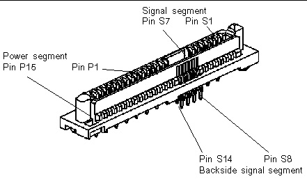
E.6 Serial Attached SCSI Connector
The Serial Attached SCSI (SAS) connector pins and their corresponding descriptions are shown in the figure and table in this section.
FIGURE E-6 Serial Attached SCSI Connector

TABLE E-6 Serial Attached SCSI Connector Pinouts
|
Segment
|
Pin Number
|
Pin Name
|
Description
|
|
Signal Segment
|
S1
|
Gnd
|
Second mate ground
|
|
S2
|
TX+
|
Positive side of transmit to hard drive
|
|
S3
|
TX-
|
Negative side of transmit to hard drive
|
|
S4
|
Gnd
|
Second mate ground
|
|
S5
|
RX-
|
Negative side of receive from hard drive
|
|
S6
|
RX+
|
Positive side of receive from hard drive
|
|
S7
|
Gnd
|
Second mate ground
|
|
|
|
|
|
|
Backside Signal Segment
|
S8
|
Gnd
|
Second mate ground
|
|
S9
|
|
Not used
|
|
S10
|
|
Not used
|
|
S11
|
Gnd
|
Second mate ground
|
|
S12
|
|
Not used
|
|
S13
|
|
Not used
|
|
S14
|
Gnd
|
Second mate ground
|
|
|
|
|
|
|
Power Segment
|
P1
|
3.3 V
|
Not used
|
|
P2
|
3.3 V
|
Not used
|
|
P3
|
3.3 V
|
Not used
|
|
P4
|
Gnd
|
First mate ground
|
|
P5
|
Gnd
|
Second mate ground
|
|
P6
|
Gnd
|
Second mate ground
|
|
P7
|
5.0 V
|
Pre-charge, second mate
|
|
P8
|
5.0 V
|
Third mate 5 V
|
|
P9
|
5.0 V
|
Third mate 5 V
|
|
P10
|
Gnd
|
Second mate ground
|
|
P11
|
Reserved
|
Not used
|
|
P12
|
Gnd
|
First mate ground
|
|
P13
|
12.0 V
|
Pre-charge, second mate
|
|
P14
|
12.0 V
|
Third mate 12 V
|
|
P15
|
12.0 V
|
Third mate 12 V
|
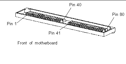
E.7 Flex Cable Motherboard Connector
The flex cable (flex circuit) motherboard connector pins and their corresponding descriptions are shown in the figure and table in this section.
FIGURE E-7 Flex Cable Motherboard Connector

TABLE E-7 Flex Cable Motherboard Connector Pinouts
|
Pin Number
|
Signal Name
|
|
1
|
DVD_DRST_L
|
|
2
|
PS1_PRESENT_L
|
|
3
|
DVD_DDATA[8]
|
|
4
|
SAS_FAN_PRSNT_L
|
|
5
|
DVD_DDATA[7]
|
|
6
|
SAS_FAN_TACH
|
|
7
|
DVD_DDATA[9]
|
|
8
|
PS1_VIN_GOOD
|
|
9
|
DVD_DDATA[6]
|
|
10
|
PS1_POWEROK
|
|
11
|
DVD_DDATA[10]
|
|
12
|
SP_I2C_DAT
|
|
13
|
DVD_DDATA[5]
|
|
14
|
SP_I2C_CLK
|
|
15
|
DVD_DDATA[11]
|
|
16
|
GND
|
|
17
|
DVD_DDATA[4]
|
|
18
|
+3.3 V AUX
|
|
19
|
DVD_DDATA[12]
|
|
20
|
PS0_PRESENT_L
|
|
21
|
DVD_DDATA[3]
|
|
22
|
PS0_ENABLE_L
|
|
23
|
DVD_DDATA[13]
|
|
24
|
SAS_FAN_LED_L
|
|
25
|
DVD_DDATA[2]
|
|
26
|
PS0_VIN_GOOD
|
|
27
|
DVD_DDATA[14]
|
|
28
|
PS0_POWEROK
|
|
29
|
DVD_DDATA[1]
|
|
30
|
DVD_DDACK_L
|
|
31
|
DVD_DDATA[15]
|
|
32
|
DVD_DRDY
|
|
33
|
DVD_DDRQ
|
|
34
|
DVD_INT_L
|
|
35
|
DVD_DDATA[0]
|
|
36
|
GND
|
|
37
|
DVD_DIOR_L
|
|
38
|
SAS_DISK3_RX_P
|
|
39
|
DVD_DIOW_L
|
|
40
|
SAS_DISK3_RX_N
|
|
41
|
DVD_DADDR[1]
|
|
42
|
SAS_DISK1_RX_P
|
|
43
|
DVD_PDIAG_L
|
|
44
|
SAS_DISK1_RX_N
|
|
45
|
DVD_DADDR[0]
|
|
46
|
GND
|
|
47
|
DVD_DADDR[2]
|
|
48
|
SAS_DISK3_TX_P
|
|
49
|
DVD_DCS1_L
|
|
50
|
SAS_DISK3_TX_N
|
|
51
|
DVD_DCS3_L
|
|
52
|
GND
|
|
53
|
DVD_DASP_L
|
|
54
|
SAS_DISK1_TX_P
|
|
55
|
+5V
|
|
56
|
SAS_DISK1_TX_N
|
|
57
|
GND
|
|
58
|
GND
|
|
59
|
SAS_DISK2_TX_N
|
|
60
|
+5V
|
|
61
|
SAS_DISK2_TX_P
|
|
62
|
GND
|
|
63
|
GND
|
|
64
|
GND
|
|
65
|
SAS_DISK2_TX_N
|
|
66
|
DISK3_ACT_LED_L
|
|
67
|
SAS_DISK0_TX_P
|
|
68
|
SPINDLE_ID0
|
|
69
|
GND
|
|
70
|
DISK2_ACT_LED_L
|
|
71
|
SAS_DISK2_RX_N
|
|
72
|
DISK1_ACT_LED_L
|
|
73
|
SAS_DISK2_RX_P
|
|
74
|
DISK0_ACT_LED_L
|
|
75
|
GND
|
|
76
|
SPINDLE_ID1
|
|
77
|
SAS_DISK0_RX_N
|
|
78
|
GND
|
|
79
|
SAS_DISK0_RX_P
|
|
80
|
PS_KILL
|
E.8 Flex Cable Power Distribution Board Connector
The power distribution board (PDB) brings power from the chassis power supplies to the motherboard. The main power connection to the motherboard is through two bus bars. The PS_KILL signals for the power supplies are grounded on the PDB to permanently enable the AUX output. The flex cable PDB connector pins and their corresponding descriptions are shown in the figure and table in this section.
FIGURE E-8 Flex Cable PDB Connector

TABLE E-8 Flex Cable PDB Connector Pinouts
|
Pin Number
|
Signal Name
|
|
1
|
PS1_PRESENT_L
|
|
2
|
PS1_ENABLE_L
|
|
3
|
SAS_FAN_TACH
|
|
4
|
PS1_VIN_GOOD
|
|
5
|
SAS_FAN_PRSNT_L
|
|
6
|
PS1_POWEROK
|
|
7
|
PDB_I2C_DAT
|
|
8
|
PS_KILL
|
|
9
|
PDB_I2C_CLK
|
|
10
|
+3.3V AUX
|
|
11
|
GND
|
|
12
|
+3.3V AUX
|
|
13
|
GND
|
|
14
|
+3.3V AUX
|
|
15
|
PS0_PRESENT_L
|
|
16
|
PS0_ENABLE_L
|
|
17
|
SAS_FAN_LED_L
|
|
18
|
PS0_VIN_GOOD
|
|
19
|
No connect
|
|
20
|
PS0_POWEROK
|
|
21
|
GND
|
|
22
|
FUSED_12V
|
|
23
|
GND
|
|
24
|
FUSED_12V
|
|
25
|
GND
|
|
26
|
FUSED_12V
|
E.9 Flex Cable DVD-ROM Drive Connector
The flex cable DVD-ROM drive IDE connector pins and their corresponding descriptions are shown in the figure and table in this section.
FIGURE E-9 Flex Cable DVD-ROM Drive IDE Connector

TABLE E-9 Flex Cable DVD-ROM Drive IDE Connector Pinouts
|
Pin Number
|
Signal Name
|
|
1
|
Audio L-CH
(not supported)
|
|
2
|
Audio R-CH
(not supported)
|
|
3
|
Audio Ground
|
|
4
|
Ground
|
|
5
|
RESET_L
|
|
6
|
DD8
|
|
7
|
DD7
|
|
8
|
DD9
|
|
9
|
DD6
|
|
10
|
DD10
|
|
11
|
DD5
|
|
12
|
DD11
|
|
13
|
DD4
|
|
14
|
DD12
|
|
15
|
DD3
|
|
16
|
DD13
|
|
17
|
DD2
|
|
18
|
DD14
|
|
19
|
DD1
|
|
20
|
DD15
|
|
21
|
DD0
|
|
22
|
DMARQ
|
|
23
|
Ground
|
|
24
|
DIOR_L
|
|
25
|
DIOW_L
|
|
26
|
Ground
|
|
27
|
IORDY
|
|
28
|
DMACK_L
|
|
29
|
INTRQ
|
|
30
|
IOCS16_L
|
|
31
|
DA1
|
|
32
|
PDIAG_L
|
|
33
|
DA0
|
|
34
|
DA2
|
|
35
|
CS1FX_L
|
|
36
|
CS3FX_L
|
|
37
|
DASP_L
|
|
38
|
+5V (Motor)
|
|
39
|
+5V (Motor)
|
|
40
|
+5V (Motor)
|
|
41
|
+5V (Logic)
|
|
42
|
+5V (Logic)
|
|
43
|
Ground
|
|
44
|
Ground
|
|
45
|
Ground
|
|
46
|
Ground
|
|
47
|
Dev Config (CSEL)
|
|
48
|
Ground
|
|
49
|
Vendor Unique
|
|
50
|
Vendor Unique
|
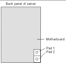
E.10 Motherboard Bus Bar Power Connector
Main power is delivered to the motherboard through a bus bar. There are two pads on the bottom side of the motherboard that connect +12 V and ground. The pads have been designed to handle 50 A. The motherboard bus bar connector pads and their corresponding descriptions are shown in the figure and table in this section.
FIGURE E-10 Motherboard Bus Bar Connector

TABLE E-10 Motherboard Bus Bar Connector Pinouts
|
Pad Number
|
Pad Name
|
Description
|
|
1
|
+12V
|
+12 VDC power to motherboard
|
|
2
|
GND
|
Ground
|
E.11 Front I/O Interconnect Cable Connector
The connection from the motherboard to the front I/O board is made through a short interconnect ribbon cable. On each board, there is a connector, Samtec STMM-113-02-S-D. The interconnect cable connector pins and their corresponding descriptions are shown in the figure and table in this section.
FIGURE E-11 Front I/O Interconnect Cable Connector

TABLE E-11 Front I/O Interconnect Cable Connector Pinouts
|
Pin Number
|
Signal Name
|
|
1
|
FAN_CTL0
|
|
2
|
FAN_CTL3
|
|
3
|
FAN_CTL1
|
|
4
|
FAN_CTL4
|
|
5
|
FAN_CTL2
|
|
6
|
FAN_CTL5
|
|
7
|
GND
|
|
8
|
GND
|
|
9
|
FRONT_USB2_N
|
|
10
|
FRONT_USB2_P
|
|
11
|
GND
|
|
12
|
GND
|
|
13
|
FRONT_LOCATE_L
|
|
14
|
+5 V
|
|
15
|
GND
|
|
16
|
GND
|
|
17
|
+5 V
|
|
18
|
+3.3 V AUX
|
|
19
|
GND
|
|
20
|
INTRUSION_SW
|
|
21
|
SP_I2C_CLK
|
|
22
|
POWER_BUTTON_L
|
|
23
|
SP_I2C_DAT
|
|
24
|
FRONT_IO_INT_L
|
|
25
|
FR_IO_PRESENT_L
|
|
26
|
VDD_RTC
|
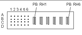
E.12 Power Supply Connector
The power supply connector pins and their corresponding descriptions are shown in the figure and table in this section.
FIGURE E-12 Power Supply Connector

TABLE E-12 Power Supply Connector Pinouts
|
Pin Number
|
Pin Name
|
Description
|
|
PB RH1
|
+12V RET
|
Main Power Return
|
|
PB RH2
|
+12V RET
|
Main Power Return
|
|
PB RH3
|
+12V RET
|
Main Power Return
|
|
PB RH4
|
+12V
|
+12 V Power Output
|
|
PB RH5
|
+12V
|
+12 V Power Output
|
|
PB RH6
|
+12V
|
+12 V Power Output
|
|
A1
|
PS_KILL
|
Turns off both main and standby outputs
|
|
A2
|
Current Share
|
Current share signal
|
|
A3
|
Return
|
Ground
|
|
A4
|
+3.3V SB
|
+3.3 V Standby Output
|
|
A5
|
PS A0
|
EEPROM Address Bit 0 Input
|
|
A6
|
+3.3V SB
|
+3.3 V Standby Output
|
|
B1
|
Return
|
Ground
|
|
B2
|
Fan_Cntl
|
Analog fan control voltage input
|
|
B3
|
Return
|
Ground
|
|
B4
|
+3.3V SB
|
+3.3 V Standby Output
|
|
B5
|
SDA
|
EEPROM Serial Data I/O
|
|
B6
|
-PS_ON
|
Enable for main supply output
|
|
C1
|
Return
|
Ground
|
|
C2
|
Tach _1
|
Fan tach output (2 pulses per rev)
|
|
C3
|
Return
|
Ground
|
|
C4
|
+3.3V SB
|
+3.3 V Standby Output
|
|
C5
|
SCL
|
EEPROM Serial Clock Input
|
|
C6
|
VIN_GOOD
|
Input voltage above minimum spec
|
|
D1
|
-PS_Present
|
Present-active low (PU)
|
|
D2
|
NC
|
No Connect (Tach_2 if two-fan design)
|
|
D3
|
Return
|
Ground
|
|
D4
|
+3.3V SB
|
+3.3 V Standby Output
|
|
D5
|
S_INT(Alert)
|
Intrusion switch alert
|
|
D6
|
POK
|
Output voltages within spec (PU)
|
E.13 Fan Module Connector
The fan module connectors and their corresponding descriptions are shown in the figure and table in this section.
FIGURE E-13 Fan Module Connector

| Note - Fan modules in Sun Fire X4100 servers each contain two 40 mm fans (Fan A and Fan B); fan modules in Sun Fire X4200 servers each contain one 80 mm fan (Fan A). The same connector is used for both types of fan modules, with slightly different assignments to connector pins, as described in TABLE E-13.
|
TABLE E-13 Fan Module Connector Pinouts
|
Pin Number
|
Pin Name
|
Description
|
|
1
|
+12V
|
+12 V power to Fan A (and to Fan B in Sun Fire X4100 fan modules)
|
|
2
|
GND
|
Ground for Fan A (and for Fan B in Sun Fire X4100 fan modules)
|
|
3
|
Fan A Tach
|
Fan A tachometer sensor
|
|
4
|
Fan B Tach
|
Fan B tachometer sensor for Sun Fire X4100 fan modules;
Presence sensor (tied to Pin 2) for Sun Fire X4200 fan modules
|
| Sun Fire X4100/X4100 M2 and X4200/X4200 M2 Servers Service Manual
|
819-1157-23
|
   
|
Copyright © 2009 Sun Microsystems, Inc. All rights reserved.


