Appendix D
Connector Pinouts
This appendix contains information about the server’s connector pinouts.
Note - The information in this appendix applies to the original Sun Fire X4600 server,
and to the Sun Fire X4600 M2 server, unless otherwise noted in the
text.
D.1 USB Connector
The USB connector pins and their corresponding descriptions are shown in the figure
and table in this section.

USB Connector Pinouts
|
|
|
|---|
1 |
+5V |
+5V supply |
2 |
Data- |
Negative side of differential for
data |
3 |
Data+ |
Positive side of differential for data |
4 |
Gnd |
Ground |
|
D.2 Serial Connector
The RJ-45 Serial connector pins and their corresponding descriptions are shown in the
figure and table in this section.

Serial Connector Pinouts
|
|
|
|---|
1 |
RTS |
Ready to send |
2 |
DTR |
Data terminal ready |
3 |
TXD |
Transmit
data |
4 |
GND |
Ground |
5 |
GND |
Ground |
6 |
RXD |
Receive data |
7 |
DSR |
Data send ready |
8 |
CTS |
Clear to send |
|
D.3 10/100BASE-T Connector
The RJ-45 10/100BASE-T connector pins and their corresponding descriptions are shown in the
figure and table in this section.

10/100BASE-T Connector Pinouts
|
|
|
|---|
1 |
TX+ |
Positive side of transmit data |
2 |
TX- |
Negative
side of transmit data |
3 |
RX+ |
Positive side of receive data |
4 |
NC |
No connect |
5 |
NC |
No connect |
6 |
RX- |
Negative side of
receive data |
7 |
NC |
No connect |
8 |
NC |
No connect |
|
D.4 10/100/1000BASE-T Connector
The RJ45 10/100/1000BASE-T connector pins and their corresponding descriptions are shown in the
figure and table in this section.

10/100/1000BASE-T Connector Pinouts
|
|
|
|---|
1 |
TP0+ |
Positive side of data pair
0 |
2 |
TP0- |
Negative side of data pair 0 |
3 |
TP1+ |
Positive side of data pair 1 |
4 |
TP2+ |
Positive side
of data pair 2 |
5 |
TP2- |
Negative side of data pair 2 |
6 |
TP1- |
Negative side of data
pair 1 |
7 |
TP3+ |
Positive side of data pair 3 |
8 |
TP3- |
Negative side of data pair 3 |
|
D.5 VGA Video Connector
The VGA video connector pins and their corresponding descriptions are shown in the
figure and table in this section.

VGA Video Connector Pinouts
|
|
|
|---|
1 |
RED |
Red video |
2 |
GRN |
Green video |
3 |
BLU |
Blue video |
4 |
ID2 |
ID2 (ground) |
5 |
GND |
Ground |
6 |
R_GND |
Red
video return (ground) |
7 |
G_GND |
Green video return (ground) |
8 |
B_GND |
Blue video return (ground) |
9 |
KEY |
No pin |
10 |
S_GND |
Sync return (ground) |
11 |
ID0 |
ID0
(ground) |
12 |
ID1/SDA |
ID1 (no connect) |
13 |
HSYNC |
Horizontal sync |
14 |
VSYNC |
Vertical sync |
15 |
ID3/SCL |
ID3 (no connect) |
|
D.6 Serial Attached SCSI Connector
The Serial Attached SCSI (SAS) connector pins and their corresponding descriptions are shown
in the figure and table in this section.
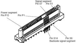
Serial Attached SCSI Connector Pinouts
|
|
|
|
|---|
|
S1 |
Gnd |
Second mate
ground |
S2 |
TX+ |
Positive side of transmit to hard drive |
S3 |
TX- |
Negative side of transmit to hard
drive |
S4 |
Gnd |
Second mate ground |
S5 |
RX- |
Negative side of receive from hard drive |
S6 |
RX+ |
Positive side of receive
from hard drive |
S7 |
Gnd |
Second mate ground |
|
|
|
|
|
S8 |
Gnd |
Second mate ground |
S9 |
|
Not used |
S10 |
|
Not used |
S11 |
Gnd |
Second mate
ground |
S12 |
|
Not used |
S13 |
|
Not used |
S14 |
Gnd |
Second mate ground |
|
|
|
|
|
P1 |
3.3 V |
Not used |
P2 |
3.3 V |
Not used |
P3 |
3.3 V |
Not used |
P4 |
Gnd |
First
mate ground |
P5 |
Gnd |
Second mate ground |
P6 |
Gnd |
Second mate ground |
P7 |
5.0 V |
Pre-charge, second mate |
P8 |
5.0 V |
Not used |
P9 |
5.0 V |
Not
used |
P10 |
Gnd |
Second mate ground |
P11 |
Reserved |
Not used |
P12 |
Gnd |
First mate ground |
P13 |
12.0 V |
Pre-charge, second mate |
P14 |
12.0 V |
Not used |
P15 |
12.0 V |
Not
used |
|
D.7 Flex Cable Motherboard Connector
The flex cable (flex circuit) motherboard connector pins and their corresponding descriptions are
shown in the figure and table in this section.

Flex Cable Motherboard Connector Pinouts
|
|
|---|
1 |
DVD_DRST_L |
2 |
DISK_ID0 |
3 |
DVD_DDATA[8] |
4 |
DISK_ID1 |
5 |
DVD_DDATA[7] |
6 |
+3.3 V |
7 |
DVD_DDATA[9] |
8 |
+3.3 V |
9 |
DVD_DDATA[6] |
10 |
+3.3
V |
11 |
DVD_DDATA[10] |
12 |
+3.3 V |
13 |
DVD_DDATA[5] |
14 |
NOT USED |
15 |
DVD_DDATA[11] |
16 |
+3.3V AUX |
17 |
DVD_DDATA[4] |
18 |
+3.3V AUX |
19 |
DVD_DDATA[12] |
20 |
+3.3V AUX |
21 |
DVD_DDATA[3] |
22 |
+3.3V AUX |
23 |
DVD_DDATA[13] |
24 |
+3.3V AUX |
25 |
DVD_DDATA[2] |
26 |
+3.3V AUX |
27 |
DVD_DDATA[14] |
28 |
Not used |
29 |
DVD_DDATA[1] |
30 |
DVD_DDACK_L |
31 |
DVD_DDATA[15] |
32 |
DVD_DRDY |
33 |
DVD_DDRQ_L |
34 |
DVD_INT_L |
35 |
DVD_DDATA[0] |
36 |
GND |
37 |
DVD_DIOR_L |
38 |
SAS_DISK1_RX_P |
39 |
DVD_DIOW_L |
40 |
SAS_DISK1_RX_N |
41 |
DVD_DADDR[1] |
42 |
SAS_DISK3_RX_P |
43 |
DVD_PDIAG_L |
44 |
SAS_DISK3_RX_N |
45 |
DVD_DADDR[0] |
46 |
GND |
47 |
DVD_DADDR[2] |
48 |
SAS_DISK1_TX_P |
49 |
DVD_DCS1P_L |
50 |
SAS_DISK1_TX_N |
51 |
DVD_DCS3P_L |
52 |
GND |
53 |
DVD_DASP_L |
54 |
SAS_DISK3_TX_P |
55 |
+5V |
56 |
SAS_DISK3_TX_N |
57 |
GND |
58 |
GND |
59 |
SAS_DISK0_TX_N |
60 |
+5V |
61 |
SAS_DISK0_TX_P |
62 |
+5V |
63 |
GND |
64 |
+5V |
65 |
SAS_DISK2_TX_N |
66 |
+5 V |
67 |
SAS_DISK2_TX_P |
68 |
+5 V |
69 |
GND |
70 |
+5
V |
71 |
SAS_DISK0_RX_N |
72 |
+5 V |
73 |
SAS_DISK0_RX_P |
74 |
+5 V |
75 |
GND |
76 |
+5 V |
77 |
SAS_DISK2_RX_N |
78 |
Not used |
79 |
SAS_DISK2_RX_P |
80 |
Not used |
81 |
PS3_PRESENT_L |
82 |
PS1_PRESENT_L |
83 |
Not used |
84 |
PS_ENABLE_L |
85 |
Not used |
86 |
PS_KILL |
87 |
Not used |
88 |
PS1_VIN_GOOD |
89 |
PS3_POWEROK |
90 |
PS1_POWEROK |
91 |
Not used |
92 |
SP_I2C_DAT |
93 |
Not used |
94 |
SP_I2C_CLK |
95 |
Not used |
96 |
Not
used |
97 |
Not used |
98 |
Not used |
99 |
PS2_VIN_GOOD |
100 |
PS0_VIN_GOOD |
101 |
Not used |
102 |
Not used |
103 |
Not used |
104 |
Not used |
105 |
PS2_VIN_GOOD |
106 |
PS0_VIN_GOOD |
107 |
PS2_POWEROK |
108 |
PS0_POWEROK |
109 |
Not used |
110 |
Not used |
111 |
Not used |
112 |
Not used |
113 |
Not used |
114 |
Not
used |
115 |
Not used |
116 |
Not used |
117 |
Not used |
118 |
Not used |
119 |
Not used |
120 |
Not used |
|
D.8 Flex Cable Power Distribution Board Connector
The power distribution board (PDB) brings power from the chassis power supplies to
the motherboard. The main power connection to the motherboard is through two
bus bars. The PS_KILL signals for the power supplies is grounded on the
PDB to permanently enable the AUX output. The flex cable power distribution board
(PDB) connector pins and their corresponding descriptions are shown in the figure and table
in this section.

Flex Cable PDB Connector Pinouts
|
|
|---|
1 |
SP_I2C_DAT |
2 |
PS1_ENABLE_L |
3 |
SP_I2C_CLK |
4 |
PS1_KILL |
5 |
GND |
6 |
+3.3 AUX |
7 |
GND |
8 |
+3.3 AUX |
9 |
GND |
10 |
+3.3 AUX |
11 |
PS0_VIN_GOOD |
12 |
PS0_POWEROK |
13 |
PS1_VIN_GOOD |
14 |
PS1_POWEROK |
15 |
PS2_VIN_GOOD |
16 |
PS2_POWEROK |
17 |
PS3_VIN_GOOD |
18 |
PS3_POWEROK |
19 |
PS0_PRESENT_L |
20 |
PS2_PRESENT_L |
21 |
PS1_PRESENT_L |
22 |
PS3_PRESENT_L |
23 |
+12 V |
24 |
GND |
25 |
+12 V |
26 |
GND |
27 |
+12 V |
28 |
GND |
29 |
+12 V |
30 |
GND |
|
D.9 Flex Cable DVD-ROM Drive Connector
The flex cable DVD-ROM drive IDE connector pins and their corresponding descriptions are
shown in the figure and table in this section.

Flex Cable DVD-ROM Drive IDE Connector Pinouts
|
|
|---|
1 |
Not used |
2 |
Not used |
3 |
GND |
4 |
GND |
5 |
DVD_RST_L |
6 |
DVD_DDATA[8] |
7 |
DVD_DDATA[7] |
8 |
DVD_DDATA[9] |
9 |
DVD_DDATA[6] |
10 |
DVD_DDATA[10] |
11 |
DVD_DDATA[5] |
12 |
DVD_DDATA[11] |
13 |
DVD_DDATA[4] |
14 |
DVD_DDATA[12] |
15 |
DVD_DDATA[3] |
16 |
DVD_DDATA[13] |
17 |
DVD_DDATA[2] |
18 |
DVD_DDATA[14] |
19 |
DVD_DDATA[1] |
20 |
DVD_DDATA[15] |
21 |
DVD_DDATA[0] |
22 |
DVD_DDRQ_L |
23 |
GND |
24 |
DVD_DIOR_L |
25 |
DVD_DIOW_L |
26 |
GND |
27 |
DVD_DRDY |
28 |
DVD_DDACK_L |
29 |
DVD_INT_L |
30 |
Not
used |
31 |
DVD_DADDR1 |
32 |
DVD_PDIAG_L |
33 |
DVD_DADDR0 |
34 |
DVD_DADDR2 |
35 |
DVD_DCS1P_L |
36 |
DVD_DCS3P_L |
37 |
DVD_DASP_L |
38 |
+5V |
39 |
+5V |
40 |
+5V |
41 |
+5V |
42 |
+5V |
43 |
GND |
44 |
GND |
45 |
GND |
46 |
GND |
47 |
GND |
48 |
GND |
49 |
Not used |
50 |
Not used |
|
D.10 Flex Cable HDD Backplane Connector
The flex cable hard disk drive backplane IDE connector pins and their corresponding
descriptions are shown in the figure and table in this section.

Flex Cable HDD Backplane IDE Connector Pinouts
|
|
|---|
1 |
SAS_DISK0_TX_N |
2 |
SAS_DISK2_TX_N |
3 |
SAS_DISK0_TX_P |
4 |
SAS_DISK2_TX_P |
5 |
GND |
6 |
GND |
7 |
SAS_DISK0_RX_N |
8 |
SAS_DISK2_RX_N |
9 |
SAS_DISK0_RX_P |
10 |
SAS_DISK2_RX_P |
11 |
GND |
12 |
GND |
13 |
DISK_ID0 |
14 |
DISK_ID1 |
15 |
+12
V |
16 |
+5 V |
17 |
+12 V |
18 |
+5 V |
19 |
+12 V |
20 |
+5 V |
21 |
+3.3 V AUX |
22 |
+5 V |
23 |
SP_I2C_CLK |
24 |
SP_I2C_DAT |
25 |
+5 V |
26 |
+5 V |
27 |
GND |
28 |
GND |
29 |
SAS_DISK1_TX_N |
30 |
SAS_DISK3_TX_N |
31 |
SAS_DISK1_TX_P |
32 |
SAS_DISK3_TX_P |
33 |
GND |
34 |
GND |
35 |
SAS_DISK1_RX_N |
36 |
SAS_DISK3_RX_N |
37 |
SAS_DISK1_RX_P |
38 |
SAS_DISK3_RX_P |
39 |
GND |
40 |
GND |
|
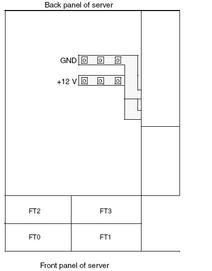
D.11 Motherboard Bus Bar Power Connectors
Main power is delivered to the motherboard through bus bar connectors that also
attach to the power distribution board. There are two connector strips that
attach to the mother board with six bus bar screws to provide +12V
and ground. See  Motherboard Bus Bar Connector for the location of the connector strips under the
motherboard.

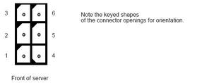
Motherboard Bus Bar Connector Pinouts
|
|
|
|---|
1 |
+12V |
+12 V DC power to motherboard |
2 |
GND |
Ground |
|
D.12 Front Flex Cable to Front I/O Board Connector
The connection from the motherboard to the front I/O board is made through
a short flex cable that is a part of the front panel indicator
board. The front flex cable connector pins and their corresponding descriptions are shown
in the figure and table in this section.

Front Flex Cable to Front I/O Board Connector Pinouts
|
|
|---|
1 |
5V_USB_D |
2 |
GND |
3 |
5V_USB_D |
4 |
FRONT_USB3_P |
5 |
5V_USB_D |
6 |
GND |
7 |
5V_USB_C |
8 |
FRONT_USB3_N |
9 |
5V_USB_C |
10 |
GND |
11 |
5V_USB_C |
12 |
Not used |
13 |
GND |
14 |
GND |
15 |
Not used |
16 |
GND |
17 |
Not
used |
18 |
GND |
19 |
Not used |
20 |
GND |
21 |
Not used |
22 |
GND |
23 |
Not used |
24 |
GND |
25 |
Not used |
26 |
Not used |
27 |
Not used |
28 |
Not used |
29 |
Not used |
30 |
Not used |
31 |
Not used |
32 |
GND |
33 |
Not used |
34 |
FRONT_USB2_P |
35 |
Not
used |
36 |
GND |
37 |
Not used |
38 |
FRONT_USB2_N |
39 |
Not used |
40 |
GND |
|
D.13 Front Flex Cable to Motherboard Connector
The connection from the motherboard to the front I/O board is made through
a short flex cable that is a part of the front panel indicator
board. The front flex cable connector pins and their corresponding descriptions are shown
in the figure and table in this section.

Front Flex Cable to Motherboard Connector Pinouts
|
|
|---|
1 |
FRONTIO_PRESENT_L |
2 |
FAN_FAIL_LED |
3 |
FRONT_USB2_N |
4 |
PS_FAIL_LED |
5 |
Not used |
6 |
OVERTEMP_LED |
7 |
FRONT_USB2_P |
8 |
POWER_BUTTON |
9 |
Not used |
10 |
POWER_LED |
11 |
Not
used |
12 |
Not used |
13 |
5V_USB_D |
14 |
+3.3 V AUX |
15 |
5V_USB_D |
16 |
Not used |
17 |
5V_USB_D |
18 |
ALERT_LED_L |
19 |
Not used |
20 |
FIO_LOCATE_L |
21 |
5V_USB_C |
22 |
P5V_AUX |
23 |
5V_USB_C |
24 |
LOCATE_LED_L |
25 |
5V_USB_C |
26 |
Not used |
27 |
Not used |
28 |
Not used |
29 |
FRONT_USB3_N |
30 |
Not used |
31 |
Not used |
32 |
Not used |
33 |
FRONT_USB3_P |
34 |
Not
used |
35 |
GND |
36 |
GND |
37 |
GND |
38 |
GND |
39 |
GND |
40 |
GND |
|
D.14 Power Supply Connector
The power supply connector pins and their corresponding descriptions are shown in the
figure and table in this section.

Power Supply Connector Pinouts
|
|
|
|---|
PB RH1 |
+12V RET |
Main Power Return
|
PB RH2 |
+12V RET |
Main Power Return |
PB RH3 |
+12V RET |
Main Power Return |
PB RH4 |
+12V |
+12
V Power Output |
PB RH5 |
+12V |
+12 V Power Output |
PB RH6 |
+12V |
+12 V Power Output |
A1 |
PS_ON |
Power supply
control |
A2 |
+12VRS_RETURN |
+12V Return remote sense |
A3 |
TEMP_OK |
Within allowable temperature range (PU) |
A4 |
PS_SEATED |
Present, active-low, short-pin (PU) |
A5 |
+3.3V SB |
+3.3
V Standby Output |
A6 |
+3.3V SB GND |
+3.3 V Standby Return |
B1 |
AC_OK |
Input voltage within spec |
B2 |
+12VRS |
+12 V
remote sense |
B3 |
+12V_ISHARE |
+12 V current-share pin |
B4 |
PS_INHIBIT |
Grounded in system to Enable, short-pin |
B5 |
+3.3V SB |
+3.3 V
Standby Output |
B6 |
+3.3V SB GND |
+3.3 V Standby Return |
C1 |
SDA |
EEPROM serial data I/O |
C2 |
SCL |
EEPROM serial clock
input |
C3 |
PWR_GOOD |
Indicates output within range |
C4 |
FAN_FAIL |
Indicates PS fan failure |
C5 |
+3.3V SB |
+3.3 V Standby Output |
C6 |
+3.3V SB
GND |
+3.3 V Standby Return |
D1 |
A0 |
EEPROM address bit 0 input |
D2 |
A1 |
EEPROM address bit 1 input |
D3 |
S_INT |
Serial
interrupt |
D4 |
+3.3V SBRS |
+3.3 V Standby remote sense |
D5 |
+3.3V SB |
+3.3 V Standby Output |
D6 |
+3.3V SB GND |
+3.3
V Standby Return |
|
D.15 Fan Module Connector
The fan module connectors and their corresponding descriptions are shown in the figure
and table in this section.

Fan Module Connector Pinouts
|
|
|---|
1 |
GND |
2 |
FAN_PWR |
3 |
FAN_TACH |
4 |
FAN_PRESENT_L |
5 |
FAN_PWM |
6 |
FAN_LED |
|


![]() Motherboard Bus Bar Connector for the location of the connector strips under the
motherboard.
Motherboard Bus Bar Connector for the location of the connector strips under the
motherboard.