| C H A P T E R 5 |
|
Hardware and Functional Description |
This chapter contains the following sections:
The Netra CP3010 board is an ATCA node board with one or two UltraSPARC IIIi processors. The card can be hot-swapped in an ATCA midplane and supports two gigabit Ethernet interfaces as Base Fabric and two gigabit SERDES interfaces as Extended Fabric to support a redundant Dual Star topology.
The Netra CP3010 board supports four Very Low Profile (VLP) DDR-1 DIMMs, which can support the maximum memory of 8 Gbytes. (For single-CPU configurations, the maximum is 4 Gbytes).
The I/O subsystem is structured around two JBus-PCI ASICs (application-specific integrated circuit), which are the bridges between the CPU JBus and the PCI buses. Each JBus-PCI ASIC has two PCI leafs, for a total of four PCI buses. The master JBus-PCI ASIC supports two PCI buses (33 MHz on the PCI-A leaf and 66 MHz on the PCI-B leaf). The slave JBus-PCI ASIC supports two 66-MHz PCI buses out of the PCI-A leaf and PCI-B leaf.
The Base Fabric interface, Extended Fabric interface, and SAS controller are connected to 66-MHz PCI leafs.
The Netra CP3010 board supports two PMC cards for PCI expansion. Both the PMC cards are interfaced with the PCI-A leaf, which is 33 MHz, 64-bit, and 5V tolerant.
The master JBus-PCI ASIC's 33 MHz leaf is used to connect the Southbridge chip. The Southbridge chip has a built-in IDE controller and supports the Compact Flash interface. The Southbridge chip provides dual RS-232 serial ports which are used for console access. These ports are available through the front as well as the rear panel.
The H8 Intelligent Platform Management controller (IPMC) requires a serial connection to communicate with SPARC host CPUs. The Southbridge chip provides a serial port, which is used to interface with the H8 controller. The Pigeon Point H8 IPMC monitors all the critical functions of the board, responds to commands from the shelf manager, and reports events. In addition, the Southbridge chip provides serial port routing to the H8 and the Base Fabric Ethernet controller for the Netconsole function.
The boot flash memory is also interfaced on the XBus. The PCI-A leaf is part of the boot path. The boot path is: JBus, master JBus-PCI PCI-A leaf, Southbridge, XBus, flash memory.
The ATCA backplane provides redundant -48V power connections, and the Netra CP3010 board derives the necessary power by using on-board DC-DC converters. Standby power is generated separately from -48V and is provided for hardware management circuitry.
FIGURE 5-1 is a block diagram of the Netra CP3010 board.
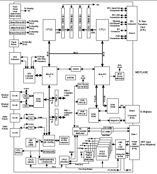
This section provides a brief description of the salient features of the UltraSPARC IIIi processor, its package, and its socket. For more extensive information on the UltraSPARC IIIi+, see the UltraSPARC IIIi Processor User's Manual at http://www.sun.com/documentation.
The UltraSPARC IIIi processor is a high-performance, highly integrated, superscaler processor implementing the 64-bit SPARC-V9 RISC architecture. It contains a 32-Kbyte instruction cache and a 64-Kbyte data cache. The chip has a built-in 1-Mbyte Level2 cache, which uses a 32-byte cache line.
The UltraSPARC IIIi processor contains a DDR-1 SDRAM memory controller, a JBus controller, and power management capabilities. The chip is housed in a 959-pin ceramic Pin Grid Array (cPGA) package. The Netra CP3010 board has an on-board socket where the UltraSPARC IIIi processor resides.
The UltraSPARC IIIi processor supports a core frequency of up to 1.8 GHz. The maximum supported JBus speed is 200 MHz, and the maximum DDR speed is 166 MHz. The CPU core speed and JBus and DDR speeds in the Netra CP3010 board depend upon the total board power budget, which cannot exceed 200W (per the PICMG 3.0 R1.0 specification).
The targeted CPU core frequency in the Netra CP3010 board is 1.06 GHz.
The UltraSPARC IIIi processor package is a 959-pin ceramic cPGA package. The pin-grid array on the chip is keyed so the chip can be inserted in the socket only in the correct orientation. The keying is accomplished by removing pin A1 from the chip and angling that corner so it does not fit in any of the other right-angle corners.
The UltraSPARC IIIi processor socket is a 959-pin ball grid array (BGA) zero-insertion-force socket. The socket is designed to be zero-insertion-force; that is, no compression is needed for the chip to make electrical contact to the pins of the socket. However, some compression (from the heatsink) is useful in keeping the module assembly in place during shock and vibration testing. Approximately 60 pounds of force is recommended for this application.
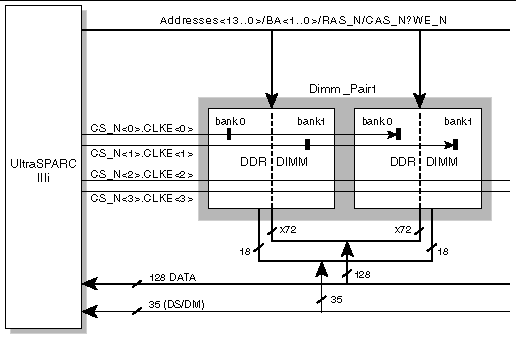
The Netra CP3010 board supports dual UltraSPARC IIIi processor CPUs, and each CPU has its own DDR memory controller. Each memory controller supports two DIMMs. Each DIMM has a 72-bit-wide data bus (64+8 ECC) and up to 14 address bits. The DIMMs run at 2.5 volts and take a 1.25 reference voltage (Vtt). PC-2100 is capable of running at up to 133 MHz.
The UltraSPARC IIIi processor defines two memory channels operating in parallel to logically create a 128-bit-wide memory data path. ECC (error correcting code) is generated and checked across 128 bits of data, allowing for significant improvement in error correction. Due to this architecture, DDR DIMMs must be installed in matched pairs.
The Netra CP3010 board can support a total of four DIMMs and a maximum memory capacity of 8 Gbytes (using 4 2-Gbyte DIMMs). The maximum memory capacity and memory speed depends upon the board's total power budget.
A DDR memory diagram is shown in FIGURE 5-2.
Some of the key features of the memory subsystem are:
All memory transfers have ECC. The UltraSPARC IIIi processor's memory controller unit (MCU) performs ECC generation and checking. A 9-bit syndrome is generated using the Hsiaos algorithm for each 128 bits of data. This 9-bit syndrome enables single-bit error correction and multiple-bit error detection.
The SQ generates the syndrome of data coming in from the JBus before it is sent to the MCU. This data is stored with the data when a write operation is performed by the MCU. When the data is read, the syndrome is also read and used to verify the correctness of the data. When a correctable or uncorrectable error is detected, the information is stored with the data and sent back to the JBus. If the data is for a foreign request, the uncorrectable error and correctable error information is sent with it on the J_ADTYPE bus.
The Netra CP3010 board supports autoconfiguration using serial presence detect (SPD). The DIMMs have small EEPROM devices that store their configuration data according to the SPD format. The OpenBoot PROM reads this data via the I2C management bus and uses it to initialize the UltraSPARC IIIi processor memory controllers.
A 128-byte region of the SPD EEPROM is available for user data storage, allowing a limited form of FRU information to be implemented for the DIMMs.
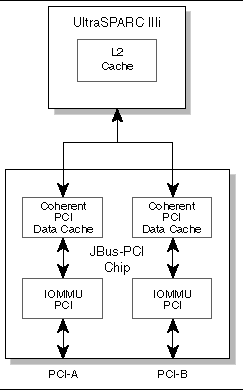
The JBus is the system bus developed for the UltraSPARC IIIi+ series processors. The JBus is the main interconnect between the CPUs and JBus-PCI ASICs. It uses 1.5V DTL signaling and is designed to run at a maximum speed of 200 MHz. The peak bandwidth for JBus is 2.56 Gbytes/sec at 200 MHz. FIGURE 5-3 is a diagram of the JBus.
JBus has a 128-bit address/data bus (J_AD[127:0]). In addition, there are several control bits that are part of the bus specification. There are 4-word parity bits (J_ADP[3:0]) for the data and address bus. An 8-bit code (J_ADTYPE[7:0]) identifies the packet type on the address and data bus. There are also encoded snoop information and flow control signals (J_PACK0-6[2:0]). The last few signals are:
There is no central system arbiter in a JBus system. Each device arbitrates for control of the bus by driving six identical output signals, J_REQ_OUT{0:5}, which are distributed to the J_REQ_IN{0:5} inputs of the remaining devices. The distribution is arranged symmetrically such that each device {i} has each of its J_REQ_IN_L{j} signals driven by the J_REQ_OUT_L{i} signals of the other devices {j}, where i and j are determined by the agent IDs. See TABLE 5-1 for the arbitration scheme.
Each device in a JBus domain is assigned a unique agent ID, J_ID{4:0}. The agent ID is a 5-bit code that defines the identity of each device in a JBus domain (TABLE 5-2). For hardware configuration, the UltraSPARC IIIi processor offers access only to the J_ID{2:0} bits, and the JBus-PCI ASICs offers access only to the J_ID{1} bit.
The UltraSPARC IIIi processor systems do not have a dedicated boot bus. The JBus-PCI ASIC 0 is defined by its agent ID as a system master and opens its PCI-1a bus as a boot path when exiting the reset state.
In the Netra CP3010 board, the boot PROM is located on the Southbridge chip XBus, which therefore occupies a position on the PCI1a bus.
JBus devices use different types of termination depending on whether they are at the center or end of the bus. The JBus architecture (reference 9) defines two types of device internal termination scheme, DTL-1 and DTL-2. Because the Netra CP3010 board has four nodes, it uses the DTL-1 scheme. Signals on the end nodes are terminated with a 50-ohm pull-up and a 50-ohm pull-down, and have the pull-up active in receive mode. Signals on the intermediate nodes are terminated with a 50-ohm pull-up and a 25-ohm pull-down, and are high-impedance in receive mode. The terminations are configured using two input pins, DOWN_25 and UP_OPEN (TABLE 5-3).
The I/O subsystem is architected around three bridges, two JBus-PCI ASICs and one 1535D+ Southbridge chip. A JBus-PCI ASICs is the bridge between the JBus and the PCI bus. The Ali1535D+ Southbridge chip is the bridge between the PCI bus and the IDE, XBus, and Super I/O functions.
The JBus-PCI ASIC is a companion core-logic ASIC to the UltraSPARC IIIi processor. The JBus-PCI ASIC and the UltraSPARC IIIi processor communicate through JBus. The central task of JBus-PCI ASIC is to be the point of access to I/O and system interrupts.
The Netra CP3010 board uses two JBus-PCI ASICs as the bridge from the JBus to the PCI. One JBus-PCI ASIC is configured as the master (JID[1]=1) and supports a 33-MHz PCI bus (PCI-A leaf) and a 66-MHz PCI bus (PCI-B leaf). The other JBus-PCI ASIC is configured as the slave (JID[1]=0) and supports two 66-MHz PCI buses through the PCI-A and the PCI-B leafs. The boot path is through the master JBus-PCI ASIC PCI-A leaf.
JBus-PCI ASIC has a built-in PCI arbiter for each leaf. The internal PCI arbiters are used for PCI arbitration. JBus-PCI ASIC's PCI-A leaf includes an interrupt block (Mondo Dispatch) that receives system interrupts from the external IChip and also deals with interrupts generated from activity within the PCI interface unit itself. The interrupt unit communicates with the JBus cluster to send the interrupt to the JBus.
This bus originates from the master JBus-PCI ASIC. It is a 33-MHz, 32/64-bit, version 2.2 compliant PCI bus. The Netra CP3010 board uses this bus to interface with two PMC slots, one Broadcom BCM5704C Ethernet controller (which provides two 10/100/1000BASE-T Ethernet ports), and the Southbridge chip (Ali1535D+). BCM5704C is a 10/100BASE-T Ethernet controller. On the Netra CP3010 board, it is used as 10/100/1000BASE-T for maintenance ports. Also, the 64-bit BCM5704C device is configured as a 32-bit device due to layout routing constraints.
The PCI-B leaf from the master JBus-PCI ASIC is 66 MHz, 64-bit, and PCI version 2.2 compliant. The SAS Controller LSISAS1064 is connected to this bus.
The PCI-A leaf from the slave JBus-PCI ASIC is 66 MHz, 64-bit, and PCI version 2.2 compliant. The BCM5704C gigabit Ethernet controller is connected on this bus. BCM5704C provides dual 10/100/1000BASE-T Ethernet ports to the ATCA backplane as a Base Fabric interface.
The PCI-B leaf from the slave JBus-PCI ASIC is 66 MHz, 64-bit, and PCI version 2.2 compliant. The BCM5704S gigabit Ethernet controller is connected on this bus. BCM5704S provides dual SERDES ports to the ATCA backplane as an Extended Fabric interace.
The Netra CP3010 board provides two Ethernet 10/100/1000BASE-T interfaces to meet the Base Fabric requirements of ATCA. The Broadcom BCM5704C Ethernet controller is used to provide dual Base Fabric interfaces. The BCM5704C is integrated MAC and GMII. These controllers are connected to the 66-MHz, 64-bit-wide PCI bus.
The controllers are magnetically coupled to the ATCA backplane for a TPE network connection. Each interface supports 10BASE-T, 100BASE-TX and 1000BASE-T operation conforming to the IEEE 802.3 specification. The controllers individually negotiate transfer speeds when their network links are established.
The Netra CP3010 board provides two gigabit Ethernet SERDES interfaces to meet the Extended Fabric requirements of ATCA in the Dual Star topology configuration. The Broadcom BCM5704S is used to provide the Extended Fabric interface. These controllers are connected to the 66-MHz, 64-bit-wide PCI bus.
The Netra CP3010 board provides two 10/100BASE-T interfaces as maintenance ports. These ports are available through the front panel or the rear transition card. A Broadcom Ethernet controller (BCM5704C) is used to provide 10/100BASE-T functions. These controllers are connected to a 33-MHz, 32-bit-wide PCI bus.
BCM5704C is an integrated Ethernet MAC, physical layer, and transceiver in one chip. The controllers are magnetically coupled to RJ-45 receptacles for a TPE network connection.
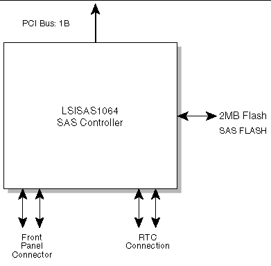
The Netra CP3010 board provides dual SAS channel ports for storage through the front panel and RTM. The LSI Logic LSISAS1064 SAS controller is used for access to high-speed storage subsystems.
The LSISAS1064 features include:
FIGURE 5-4 is a block diagram of the SAS controller.
The Netra CP3010 board provides two 64-bit, 33-MHz PMC slots for PCI expansion. The PMC interface is designed to support PIM for rear I/O access availability. The Netra CP3010 board supports 5V PMC modules, and the slots are keyed accordingly. The maximum power consumption supported for each PMC slot is 7.5W.
The Netra CP3010 board uses the ALi M1535D+ Southbridge chip from Acer Labs. M1535D+ is a highly integrated system I/O chipset in a 328-pin BGA package. The following functions of Southbridge are used on the Netra CP3010 board:
The Southbridge chip is interfaced on a 33-MHz, 32-bit PCI leaf.
The ISA bus is an I/O bus that runs at 8 MHz. The Netra CP3010 board uses only a subset of this bus, called XBus. The OpenBoot PROM flash, SRAM, XBUS CPLD, and real-time clock are interfaced onto the XBus.
The Netra CP3010 board provides two serial ports using Southbridge chip super I/O functions. Both the serial ports are available for front as well as rear access. The COM1 port is the output to the netconsole utility. When a serial port cable is connected to the front or rear COM1 port, netconsole is disabled and the signal passes through the standby CPLD. Without a serial port cable connected, the serial port output from the Southbridge chip is redirected to netconsole through the H8S. The MAX3243 RS-232 transceivers are used for these serial interfaces. The MAX3243 provides the required ESD protection to the serial ports.
FIGURE 5-5 shows a block diagram of the serial interface.
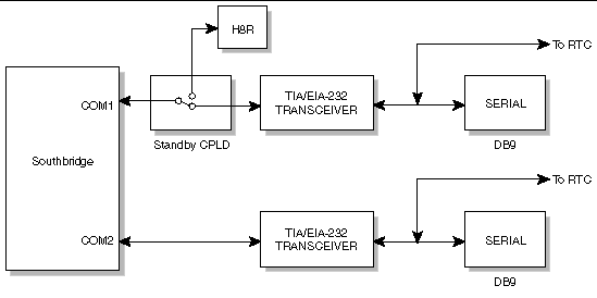
The Southbridge chip provides one additional two-wire serial port. This is used to interface with the IPMB controller BMR-H8S. This interface is referred to as the payload interface, and enables messaging between the SPARC and management interface.
The M1535D+ provides an XBus controller. XBus is an 8-bit, parallel interface provided by the Southbridge chip for general use in supporting ISA style devices.
In the Netra CP3010 board, the XBus is used to interface with the flash, SRAM, XBus CPLD, and real-time clock (M5823), as seen in FIGURE 5-6.
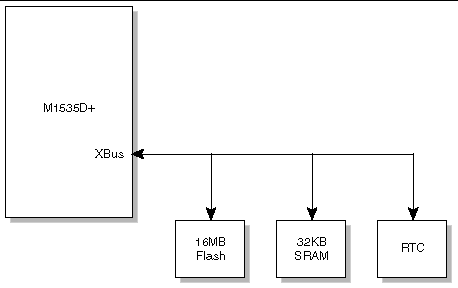
The Southbridge chip provides chip selects for these devices, as detailed in TABLE 5-4.
|
Internal to the XBus CPLD to control the FLASH paging mechanism |
||
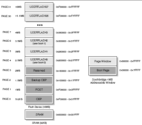
The flash PROM and SRAM devices are used by the OpenBoot PROM and POST. The PROM is a 16-Mbyte flash device. Two Mbytes contain the OpenBoot PROM, OpenBoot Diagnostics, and POST firmware suites. The SRAM is a 32-Kbyte device available to OpenBoot PROM and POST for storage of temporary variables. Following a system reset, the Southbridge chip provides a boot path to the PROM to run the OpenBoot PROM system initialization code.
As a result of enabling parallel interrupts (APIC mode) within the Southbridge chip, the most significant bit (msb) of the XBus address bus is unavailable on the XA19 pin. In the Netra CP3010 board, XA19 is therefore obtained by latching PCI_AD19 directly from the PCI bus, using the first PCI clock pulse after the FRAME# signal is asserted.
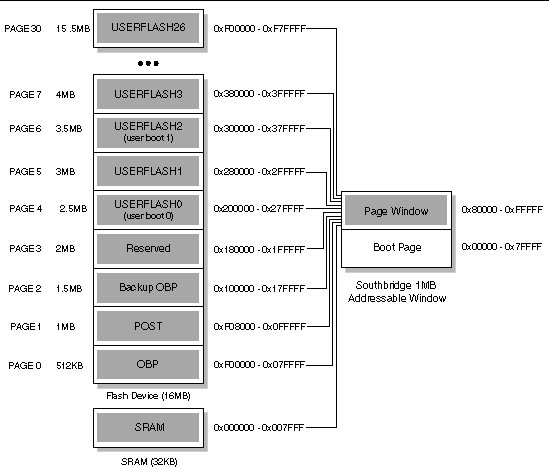
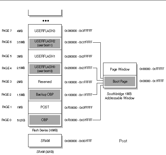
For the Netra CP3010 board, a 16-Mbyte flash device is addressed. This is accomplished by breaking up the 1-Mbyte Southbridge chip addressable window into two 512-KBytes segments. The lower segment always addresses a boot block of 512 Kbytes, whereas the upper segment can page in any of the 32 512-Kbyte pages in the flash device. The lower segment boot block can be at the 0-Mbyte, 1-Mbyte, 2-Mbyte, or 3-Mbyte offset, which is controlled by the IPMC. The lower segment is protected from write operations at all times. (If writing a boot page, it must be mapped to the upper 512 Kbytes.) In case of a flash-update failure, or a need to allow booting from userflash, the IPMC can control which of the four boot pages is selected. The upper segment can page in any of the 32 pages (including boot pages).
SRAM is mapped to upper 16M-32K (0xFF8000-0xFFFFFF). To access SRAM, SRAMEN GPIO 34 from the Southbridge chip must be set high and the CPLD register's page window must be set to page 31. FIGURE 5-7 shows the XBus memory map, FIGURE 5-8 shows the page window address aliasing map, and FIGURE 5-9 shows the boot page address aliasing map.
The Solaris OS uses the real-time clock (RTC) as its reference source for calendar date and time. Under normal circumstances, synchronization occurs once at boot time, after which the processors maintain an internal record using their STICK counters.
The Netra CP3010 board uses an Acer M5823 device for RTC functions. The M5823 is a full BDC clock and calendar. The real-time clock counts seconds, minutes, hours, date of month, month, day of week, and year, with leap year compensation.
A battery provides the backup power to the RTC when power is not present.
The IDE controller is an Acer M5229 device that resides inside the M1535D+ Southbridge chip. This is a dual controller, but only the primary bus is utilized to connect the Compact Flash card in the Netra CP3010 board. The bus can operate at DMA mode 4 speed. At the present time, direct memory access (DMA) is a new enhancement to the Compact Flash specification, and the majority of Compact Flash cards use programmed I/O (PIO). There is a performance impact compared to a normal IDE disk.
A Southbridge chip GPIO pin connects to an interrupt input pin of the H8. This enables OS-level interrupts to be sent to the H8 due to the limitations of the watchdog within the H8 (primarily, insufficient time resolution).
GPO29 from the Southbridge chip is used to connect to /IRQ0 on the H8.
The Netra CP3010 board provides the option of supporting an IDE Compact Flash (CF) card. To support higher memory capacity, a Type I CF socket is provided. The Compact Flash card is not hot-swappable and there is no access to the CF socket once the board is installed in an ATCA chassis.
The Southbridge chip GPIO pins are configured for the uses summarized in TABLE 5-5. Further description of the signal usage can be found in the relevant sections of this specification.
The Renesas H8S/2168 provides the IPM controller (IPMC) function on the Netra CP3010 board. The IPMC provides PICMG 3.0 board management functionality, and it interfaces to the payload through a serial interface.
The IPMC is responsible for the following:
The IPMC communicates with the SPARC chip through the serial interface, which connects to the M1535D+ Southbridge (COM3). The interface protocol is SIPL (Serial Interface Protocol Lite), which is based on the IPMI-defined basic mode of the serial/modem interface. The baudrate supported is 9600 bps.
The IPMC provides dual buffered IPMB interfaces to the IPMB-0 bus on the PICMG 3.0 backplane. The I2C channels on the IPMC are connected to the IPMB-A and IPMB-B through the LTC4300A I2C buffers. The I2C buffers enable the board's I2C to be isolated from the backplane until the board is fully seated and the I2C bus on the backplane is idle.
Hot-swapping is supported by monitoring of the hot-swap handle switch and LED control. The handle switch goes directly to one of the GPIO pins on the IPMC. The LEDs are controlled through the memory mapped registers on the standby complex programmable logic device (CPLD).
The IPMC is able to control individual power rails to the payload. This is accomplished through the memory mapped registers in the standby CPLD.
The IPMC provides E-Keying for the payload interfaces to the backplane. PICMG mandates that the software hooks for E-Keying are present, but it does not mandate that anything must be done in hardware in response. There is no hardware support for E-Keying in the Base Fabric interfaces. E-Keying for the Fabric interfaces is accomplished by setting the SIG_DET lines active into the BCM5704S. This is done through memory mapped registers in the standby CPLD.
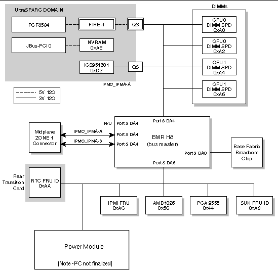
Both IPMI and Sun FRU information (FRU IDs) are supplied. IPMI FRU information is supported through an 8-Kbyte serial EEPROM (AT24C64B) on the system management I2C bus. The Sun FRU information is supported through an additional 8-Kbyte serial EEPROM.
The IPMC serial port 0 connects to the serial port on the Southbridge chip through the standby CPLD. The standby CPLD provides the appropriate control to enable this serial port to be routed either to the front or back (when a connection is detected on either of these ports). If there is no connection to the front or rear serial port, this serial port is routed to the H8 and from there to the Base Fabric chipset to enable Netconsole functionality.
The IPMC I2C port 0 is used to connect to the Broadcom chipset for the Base Fabric interface.
The Analog Devices ADM1026 is used for system monitoring functions. The ADM1026 is interfaced with the IPMC and the IPMC firmware is responsible for monitoring these sensors.
The ADM1026 measures most of the board voltages. The ADM1026 has one temperature sensor embedded in the device itself and supports two remote sensing channels that require external diodes for temperature sensing. These two remote sensors are used for measuring CPU die (or junction) temperatures.
The ADM1026 measures the voltages listed in TABLE 5-6. The ADM1206 and H8 firmware monitors these voltages. When the voltages are within regulations, the board functions with no warnings. When any voltage goes out of regulation beyond approximately ± 7%, a Critical Warning is generated and presented to the shelf manager. When any voltage goes out of regulation beyond approximately ± 10%, the H8 initiates a board shutdown.
Also shown in TABLE 5-6 are voltage shutdown limits set by hardware components on the Netra CP3010 board itself. In addition to the H8 shutdown, these on-board components monitor certain voltage rails and force a shutdown whenever any of these voltages go beyond the On Board Hardwired Shutdown voltage.
The ADM1026 also monitors the CPU die (or junction) temperatures of each CPU on the Netra CP3010 board. The ADM1206 and H8 firmware reports a minor, major, or critical alarm when the temperature of either CPU goes beyond the thresholds listed in TABLE 5-7. Also, if the temperature of either CPU goes beyond the Emergency H8 Shutdown value listed in TABLE 5-7, the H8 initiates a board shutdown independent of the shelf manager.
The H8 temperature alarm equivalents are:
Minor Alarm = Upper Non Critical (UNC)
Major Alarm = Upper Critical (UC)
Critical Alarm = Upper Non Recoverable (UNR)
Emergency H8 Shutdown = Emergency H8 Shutdown (EMR)

|
Caution - These voltage and temperature thresholds should not be changed under normal operating conditions. |
FIGURE 5-10 is a block diagram of the I2C architecture.
As shown in FIGURE 5-11, all the interrupts are delivered to the UltraSPARC IIIi processor through dedicated JBus transactions. These transactions are identical to the interrupt packets defined by Sun architecture.
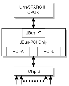
In the Netra CP3010 board, the Sun IChip2 receives all the system interrupts and encodes the interrupts into a 6-bit interrupt vector. The interrupt vector is then issued to the JBus-PCI ASIC. The JBus-PCI ASIC issues a single JBus transaction for each active interrupt to the UltraSPARC IIIi processor.
The BMR-H8S interrupt IRQ0 is also connected to the Southbridge chip to enable the OS to interrupt the H8. Its use is left to the software application running on the H8.
Interrupts are delivered to the processors through dedicated transactions on the JBus. These transactions employ the interrupt packets defined by the Sun architecture. The packet includes the agent ID of the JBus source, the agent ID of the JBus target, and the source of the interrupt. Interrupt packets for I/O devices and for JBus or PCI bus errors are issued by the JBus-PCI ASICs. The processors can also initiate interrupts to each other. These interrupts are known as cross-calls.
In the Netra CP3010 board, the Sun IChip ASIC is used as an interrupt concentrator, receiving all hardware interrupts and passing them to the JBus-PCI ASICs for conversion to JBus packets. The IChip samples its discrete interrupt inputs on a round-robin basis and submits the results of each sample to the JBus-PCI ASICs in sequential format. Each interrupt is encoded as a 6-bit vector. An idle code is passed when no interrupt is detected. FIGURE 5-12 is a diagram of the IChip.
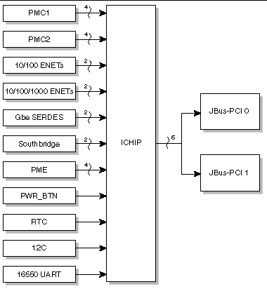
The IChip has two types of interrupt input, level interrupts and pulse interrupts. Only level interrupts are used in the Netra CP3010 board. Most level interrupt inputs are active-low, but four active-high inputs are included for legacy support.
Each 6-bit vector uniquely defines the interrupt source device and translates to the interrupt number offset (INO) used in the JBus packet. TABLE 5-8 shows the I/O device interrupt sources.
In the Netra CP3010 board, the Southbridge chip interrupt controller must be configured for APIC mode. This enables individual interrupts to be accessed on discrete pins of the Southbridge chip, rather than multiplexed onto a single serial line. Internal devices are each allocated to appropriate interrupts as part of the configuration process. The Southbridge chip has the capability to provide 10 interrupts. In the Netra CP3010 board, only two are used. TABLE 5-9 lists the Southbridge chip interrupts.
The IChip interrupt vectors are passed to both JBus-PCI ASICs in parallel. A JBus-PCI ASIC processes an interrupt only if the source is recognized as belonging to one of its PCI leaves. To achieve this, the JBus-PCI ASIC has an Interrupt Routing Register and an Interrupt Mapping Register. These registers are initialized by the OpenBoot PROM to assign ownership of individual interrupt sources to the correct JBus-PCI ASIC and PCI leaf.
When a JBus-PCI ASIC recognizes an IChip interrupt vector, it dispatches an interrupt packet to the JBus. The packet defines the interrupt source in an 11-bit field known as the interrupt number (INR). The INR is composed of the interrupt group number (IGN), which specifies the JBus agent ID, and the interrupt number offset (INO), which corresponds to the IChip vector.
The JBus-PCI ASIC provides a state machine for each level interrupt assigned to it. The state machine has three states: idle, received, and pending. The state machine moves from the idle to received state when an assigned interrupt is recognized. Once the corresponding interrupt packet has been dispatched to the JBus, the state machine moves to the pending state. The pending state prevents further interrupt packets from being generated each time the IChip round-robin cycle returns to the same interrupt source. As part of the interrupt routine, the servicing processor must both clear the IChip interrupt by writing to the appropriate register in the source device, and return the JBus-PCI ASIC state machine to the idle state by writing to the corresponding JBus-PCI ASIC Clear Interrupt Register.
The JBus-PCI ASICs implement error checking on the JBus transfers. In addition, they respond to bus errors on the JBus and on each of their PCI buses. These errors are converted to interrupts and dispatched as JBus packets in exactly the same way as IO device interrupts. TABLE 5-10 shows the JBus-PCI ASIC error interrupts.
The H8/IRQ0 interrupt input is connected to a GPIO pin (GPO29) to enable the OS to interrupt the H8. The use of this interrupt is left to the application running on the H8.
The Netra CP3010 board supports two different types of resets, which can be triggered by several different methods. The two main types of resets are hard resets and soft resets.
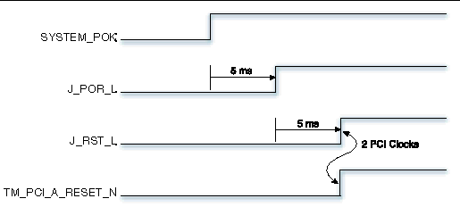
There are two ways to cause a hard reset. The first is when the system powers on and asserts the SYSTEM_POK signal, which connects to the PWRGD pin on the Master JBus-PCI ASIC and causes a hard reset. The JBus-PCI ASIC then asserts the J_POR_L and J_RST_L signals for 5 milliseconds (ms). The J_RST_L signal is kept asserted for 5 ms after the deassertion of the J_POR_L signal. The PCI reset pins are kept asserted until after the deassertion of the J_RST_L signal. This causes the entire system to reset.
A hard reset can also be generated by software. The CPU writes to the JBus-PCI ASIC to initiate a reset. This reset is similar to the hardware-initiated hard reset, except the JBus-PCI ASIC's clock PLLs are not reset. The Reset Source, Estar Control, Estar Init, and PCI PIO AFSR registers in the JBus-PCI ASIC preserve their state across the reset.
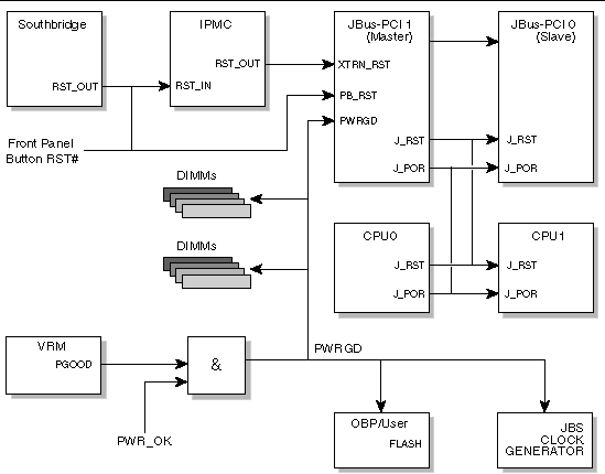
There are two different types of hard resets. In a long reset, J_POR_L and J_RST_L signals are asserted for 5 ms. In a short reset, J_POR_L is asserted for 32 JBus clocks and J_RST_L is asserted for 64 JBus Clocks. For the Southbridge chip, all hard resets must be long resets. FIGURE 5-13 is the block diagram and FIGURE 5-14 is the timing diagram for hard rests.
A soft reset is different from a hard reset in that the memory controller in the UltraSPARC IIIi processor continues to refresh memory to preserve the contents of the memory. The clock ratios for the CPUs are unaffected by a soft reset. The PCI resets are also generated during a soft reset.
The Netra CP3010 board provides three possible sources for the soft reset in hardware, as well as a software-generated soft reset. Other than their origin, there is no difference between any of these resets.
Three hardware soft resets are generated by the host:
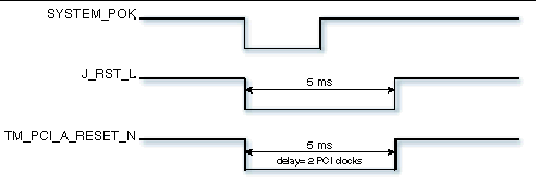
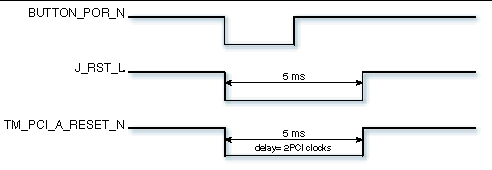
When any of the external events asserts the PB_RST input of JBus-PCI ASIC or when software issues a soft reset of the host, the J_RST_L signal is driven low for 5 ms (see FIGURE 5-15). This resets all the CPUs in the system. One or two PCI-clocks later the PCI resets are asserted, resetting the rest of the devices in the payload.
The XIR function on the Netra CP3010 board restarts a hung system without resetting it so that information can be retrieved from memory for analysis. An XIR can be initiated by pulsing the XTRN_RST# input of the master JBus-PCI ASICs (see FIGURE 5-16).
There are three ways to issue an XIR to the system. The first way is through setting a bit in the JBus-PCI ASIC that generates an XIR to the CPUs. The IPMC can also issue an XIR using the same input pin. The last method is using the watchdog timer. The watchdog timer can be set to generate either a reset or an XIR when a watchdog timeout occurs.
When power is first turned on to the system, the PCI reset deasserts until the JBus-PCI ASIC begins operating. This is in violation of the PCI spec and can cause issues with PCI devices. The solution is to gate the PCI resets with the SYSTEM_POK signal, which ensures that the reset signal is held low until the JBus-PCI chip brings the system out of reset.
PCI devices are reset by signals from the JBus-PCI ASICs. Each JBus-PCI ASIC generates a separate reset signal for each of its PCI buses. The JBus-PCI ASIC asserts the PCI reset signals during a POR event.
Because the Southbridge chip is the source of PCI resets in the PC architecture, it does not have a PCI reset input. In the Netra CP3010 board, the Southbridge chip receives PCI resets via its PWG input. The Southbridge chip requires a delay of at least 2.5 ms after the reset is negated before the OpenBoot PROM can be accessed.
The delay is produced by implementing the Southbridge chip reset as a nominal 1.2 ms pulse at the leading edge of the PCI reset, derived from the 32.768 kHz resume clock. The P_RST# signal of the master JBus-PCI ASIC is used as the source of the reset. To meet the 2.5 ms requirement, this reset must be programmed for its maximum duration.
During the power on initialization sequence, the 2.5 ms requirement is met automatically because the master JBus-PCI chip delays release of the JBus from reset until after the PCI reset signals are negated. The PWRGD signal is therefore fed directly to the Southbridge PWG input at power-on.
The host software can reset the IPMC at any time by generating a low-going pulse on the GPO39 pin of the Southbridge chip. This pin connects to the IPMC_RST# signal.
The IPMC is also able to reset the host system by generating a low-going pulse on the RST_OUT# pin of the H8. This is connected to XTRN_RST# input of the master JBus-PCI chip and causes soft reset.
A software-initiated reset (SIT) is triggered by execution of an SIR instruction. An SIR resets only the processor that executes the instruction and has no effect on the remaining system.
If a processor tries to take a trap when the trap level is already at its maximum value (TL=MAX_TL), an error is generated, resulting in a watchdog reset (WDR). A WDR resets only the processor that executes the instruction and has no effect on the remaining system.
TABLE 5-11 gives fundamental clock sources in the Netra CP3010 board. All are referenced from crystal sources. Other clocks within the system are derived from these crystal sources by synthesis or division.
All JBus devices in the system share a common clock. This is a low-voltage PECL signal generated by a Motorola MC9229FA clock generator and distributed by a Motorola MC100ES6014 phase-locked loop. FIGURE 5-17 shows a block diagram of the JBus Clock.
The JBus clock speed is determined by the MC9229FA, which synthesizes the desired frequency, Fout, from a 16-MHz crystal source, Fxtal, and programmable constants M and N, according to the formula:
where M is a 9-bit binary code taking values from 200 to 400, and N is a 2-bit geometric code.
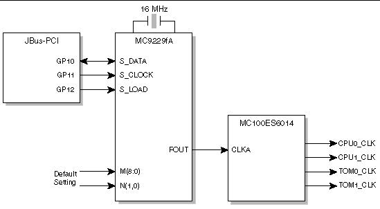
The MC9229FA provides both parallel and serial interfaces for programming its M and N values. Following a power-on reset, the initial frequency is determined by the M and N settings programmed at the parallel interface. During system initialization, the serial interface is used to update the M and N values to reflect the actual required operating frequency appropriate for the speed grades of the components fitted. The serial interface is constructed from the GPIO{2:0} pins of the slave JBus-PCI ASIC. The GPIO pins must be "bit-banged" by the OpenBoot PROM to simulate the required transfer protocol for the MC9229FA.
The UltraSPARC IIIi processor contains internal phase-locked loops that synthesize clocks for the CPU core and the memory controller from the input JBus clock. The synthesizers have programmable ratios that can accommodate a wide variety of clock conditions (see FIGURE 5-18).
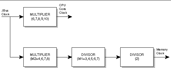
TABLE 5-12 lists the clock frequencies.
The required system clock operating frequencies are set by configuration parameters stored in a look-up table in the FRU ID EEPROM on the motherboard.
In the Netra CP3010 board, the default frequency is set to 120 MHz, the minimum supported operating frequency of the JBus chipset. This frequency enables all systems to initialize from the same default setting, regardless of the speed grades of the components. The default value is determined by the M and N values configured at the parallel interface of the MC12429. TABLE 5-13 gives the JBus default clock frequencies.
Once the OpenBoot PROM has determined the actual operating frequency from the motherboard FRU ID EEPROM, the MC9229FA M and N values are revised via the serial interface.
Sudden disturbances in the output of the MC9229FA might cause instability in the various phase-locked loops, resulting in a crash. To prevent this, make changes to the JBus frequency progressively in 1-MHz steps.
The STICK clock is a 12-MHz crystal oscillator. The STICK clock is provided primarily to allow the processors to maintain an internal source of real time. The crystal oscillator accuracy should be better than 25 ppm at 25oC, which equates to 2.16 seconds of error per day.
Each processor has a STICK input. The SPARC V9 architecture defines a system "tick" counter that provides a synchronized system-wide clock source for use by software applications. The counter provides a way to accurately time stamp multithreaded programs. The STICK timer is initialized from the RTC during boot, after which real time is maintained by counting overflows of the "tick" counter.
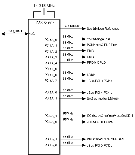
PCI clocks for devices on the four PCI buses are generated by an ICS951601 clock synthesizer with a 14.318-MHz crystal source. This device also generates two reference clocks for the Southbridge chip. Each of the four PCI buses has its own clock group operating at the appropriate frequency.
The ICS951601 is accessible through the I2C management bus. This enables the OpenBoot PROM to turn off individual clocks to the PCI slots if cards are not detected when these slots are probed. FIGURE 5-19 is a block diagram of the PCI device clock.
The RTC clock operates from a 32.768-kHz crystal. This is provided by a small crystal on the board. To allow the RTC to maintain representative real time, the crystal accuracy should be better than 20 ppm at 25oC. This equates to 1.728 seconds of error per day.
Each Ethernet controller operates from a 25-MHz crystal. There are three Ethernet controllers on the board. To maintain adequate network timing performance, the crystal accuracy should be better than 20 ppm at 25oC. Cypress Programmable clock generator CY2205 is used to generate 25-MHz Ethernet clocks and the 12-MHz STICK clock.
The SAS controller requires a 40-MHz clock. This is provided using a crystal oscillator. The accuracy requirement for this clock is 25 ppm at 25oC.
The BMR-H8S operates from a 7.3728-MHz crystal oscillator.
The Netra CP3010 board is powered from dual-redundant -48V power supply inputs from the backplane power connector (P10). The Netra CP3010 board takes redundant -48V as input and derives the other necessary power using DC-DC converters. The Netra CP3010 board design complies with the ATCA power distribution specification and includes:
As required by the PICMG 3.0 R1.0 specification, the Netra CP3010 board provides fuses on each of the -48V power feeds and on the return (RTN) connections. The fuses on the return feeds are critical to protect against overcurrent when an ORing diode in the return path fails. There are eight fuses on board and connections to -48V_A, -48V_B, RET_A, RET_B, EARLY_A, EARLY_B, ENABLE_A, and ENABLE_B power feeds. The fuses are single-blow type and must be replaced when blown.
The Netra CP3010 board uses the Artesyn ATCA power module solution. The Artesyn power module provides an integrated ATCA power solution that meets PICMG 3.0 requirements, including dual bus input, DC isolation, hold up, hot plug, and management power (3.3V standby). It provides a 12V intermediate bus as backend power. Some of the salient features of the module are:
The Netra CP3010 board uses Point-of-Load Alliance (POLA) compatible power modules for generating other on-board power requirements. All the voltages are generated from +12V input power. TABLE 5-14 provides Sun part numbers and manufacturing part numbers.
The UltraSPARC IIIi processor takes 1.2V for its internal core logic. An Artesyn Haymaker50 SIP module is used to generate CPU core power. The operating characteristics are:
DDR memory requires 2.5V, which is also generated by POLA module PTH12030WAH. The operating characteristics are:
All the DTL I/O power (1.5V) is generated using POLA module PTH12060WAH and delivered to CPUs and JBus-PCI ASICs for the DTL I/O. The operating characteristics are:
The PTH12060YAH POLA module is used to provide the termination voltage (1.25V) for all the DDR memory interface signals. It should be set to 1.25V output and should be tracking the DC variation of VDDQ. The operating characteristics are:
The PTH12050WAH POLA module is used to provide the +2.5V power for the JBus-PCI ASIC core only. Both the JBus-PCI ASICs are powered from a single power converter. The operating characteristics are:
All the Ethernet controllers (Broadcom BCM5704C or BCM5704S) need 1.2V as core power, 2.5V analog supply voltage, and 3.3V for PCI. The 1.2V core power and 2.5V analog power are derived from 3.3V using a Broadcom built-in power converter.
The SAS controller requires 1.2V core power. The LTC1772 is used to generate 1.2V core power for SAS. The output voltage is generated from 3.3V.
Copyright © 2006, Sun Microsystems, Inc. All Rights Reserved.