Appendix C Functional Description
This appendix provides a functional description for the following:
The following items are not supported on the Sun Enterprise 220R server:
-
Graphics and imaging card
-
Diskette drive
-
Audio card
C.1 System Unit
The system unit is an UltraSPARC port architecture (UPA)-based multiprocessor machine that uses peripheral component interconnect (PCI) as the I/O bus. The CPU modules, U2P ASIC (UPA-to-PCI bridge), and UPA graphics cards communicate with each other using the UPA protocol. The CPU modules and the U2P ASIC are UPA master-slave devices. The UPA graphics cards are UPA slave-only devices. The QSC ASIC routes UPA request packets through the UPA address bus and controls the flow of data using the XB9+ ASIC. For further information, see the following items:
The following figure shows the system unit functional block diagram.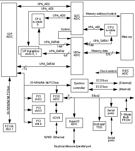
C.1.1 UPA
The UltraSPARC port architecture (UPA) provides a packet-based interconnect between the UPA clients: CPU modules, U2P ASIC, and UPA graphics cards. Electrical interconnection is provided through four address buses and four data buses.
The four address buses are:
-
UPA address bus 0 (UPA_AD0)
-
UPA address bus 1 (UPA_AD1)
-
UPA address bus 2 (UPA_AD2)
-
UPA address bus 3 (UPA_AD3)
The four data buses are:
-
UPA data bus 0 (UPA_DATA0)
-
UPA data bus 1 (UPA_DATA1)
-
UPA data bus 2 (UPA_DATA2)
-
UPA data bus 3 (UPA_DATA3)
UPA_AD0 and UPA_AD1 connect the QSC ASIC to the CPU modules and the U2P ASIC. UPA_AD2 connects the QSC ASIC to the U2P ASIC. UPA_AD3 connects the QSC ASIC to the UPA graphics.
Two processor data buses (UPA_DATA0 and UPA_DATA1) are bidirectional 144-bit data buses (128 bits of data and 16 bits of ECC) that connect each CPU module to the XB9+ ASIC. The I/O data bus is a bidirectional 72-bit data bus (64 bits of data and 8 bits of ECC) that connects the U2P ASIC and the UPA graphics (UPA_DATA2) to the XB9+ ASIC (UPA_DATA3). The UPA graphics do not have ECC, and therefore only consists of 64 bits of data.
The following table illustrates UPA slot number port addresses.
|
UPA Slot Number |
UPA Port ID <4:0> |
|---|---|
|
CPU module slot 0 |
0x0 |
|
CPU module slot 1 |
01 |
|
U2P ASIC |
0x1F |
The following figure shows the data buses functional block diagram.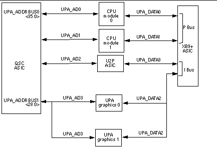
C.1.2 PCI Bus
The peripheral component interconnect (PCI) bus is a high-performance 32-bit or 64-bit bus with multiplexed address and data lines. The PCI bus provides electrical interconnection between highly integrated peripheral controller components, peripheral add-on devices, and the processor/memory system.
There are two PCI buses. The first bus is a one-slot, 3.3-VDC, 64-bit or 32-bit, 66-MHz or 33-MHz bus. The second bus is a three-slot, 5.0-VDC, 64-bit or 32-bit, 33-MHz bus. Each bus is controlled by the UPA-to-PCI bridge (U2P) ASIC. There are also two on-board controllers, the Symbios 53C876 SCSI controller and the PCI-to-Ebus/Ethernet controller (PCIO) ASIC, on the 33-MHz PCI bus.
C.1.2.1 U2P ASIC
The UPT-to-PCI bridge (U2P) ASIC controls the PCI buses. It forms the bridge from the UPA bus to the PCI buses. For a brief description of the U2P ASIC, see "C.1.12 ASICs".
C.1.2.2 Symbios 53C876 SCSI Controller
The Symbios 53C876 SCSI controller provides electrical connection between the main logic board and the internal and external SCSI buses to the PCI bus. The Symbios controller is two SCSI controllers on the same PCI slot. Controller "A" is used to interface to internal devices. The second controller, controller "B," is used to interface to external devices.
C.1.2.3 PCIO ASIC
The PCI-to-EBus/Ethernet controller (PCIO) ASIC bridges the PCI bus to the EBus, enabling communication between the PCI bus and all miscellaneous I/O functions, as well as the connection to slower on-board functions. The PCIO ASIC also embeds the Ethernet controller.
C.1.3 UltraSPARC II Processor
The UltraSPARC II processor is a high-performance, highly-integrated superscalar processor implementing the SPARC-V9 64-bit RISC architecture. The UltraSPARC II processor is capable of sustaining the execution of up to four instructions per cycle even in the presence of conditional branches and cache misses. This sustained performance is supported by a decoupled prefetch and dispatch unit with instruction buffer.
The UltraSPARC II processor supports both 2D and 3D graphics, as well as image processing, video compression and decompression, and video effects through the sophisticated visual instruction set (VIS). VIS provides high levels of multimedia performance, including real-time video compression/decompression and two streams of MPEG-2 decompression at full broadcast quality with no additional hardware support. The UltraSPARC II processor provides a 2-Mbyte ecache, with an 300-MHz operating frequency.
UltraSPARC II processor characteristics and associated features include:
-
SPARC-V9 architecture compliant
-
Binary compatible with all SPARC application code
-
Multimedia capable visual instruction set (VIS)
-
Multiprocessing support
-
Glueless four-processor connection with minimum latency
-
Snooping cache coherency
-
Four-way superscalar design with nine execution units; four integer execution units
-
Three floating-point execution units
-
Two graphics execution units
-
Selectable little- or big-endian byte ordering
-
64-bit address pointers
-
16-Kbyte non-blocking data cache
-
16-Kbyte instruction cache; single cycle branch following
-
Power management
-
Software prefetch instruction support
-
Multiple outstanding requests
C.1.4 Memory System
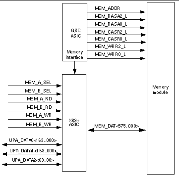
The memory system consists of three components: the QSC ASIC, the XB9+ ASIC, and the memory module. The QSC ASIC generates memory addresses and control signals to the memory module. The QSC ASIC also coordinates the data transfers among the DIMMs through two 144-bit-wide processor data buses (UPA_DATABUS0) and the 72-bit-wide I/O data bus (UPA_DATABUS1).
DIMMs are organized in banks in groups of four (quads). DIMM capacities of 32-Mbyte, 64-Mbyte, and 128-Mbyte are supported by the memory module. When all DIMM banks are populated with 128-Mbyte DIMMs, maximum memory capacity is 2 Gbytes.
Organizing the four DIMM banks with 128-Mbyte (plus ECC bit) DIMMs allows data streams to be transferred on a 512-bit-wide (plus ECC) memory data bus. The XB9+ ASIC coordinates all buses, which include the following: memory data, UPA_DATA0, UPA_DATA1, UPA_DATA2, and UPA_DATA3.
The memory module is arranged in four banks. DIMMs are always accessed four at a time. Consequently, the DIMMs must be installed in groups of four (quad) and individual DIMMs within a bank must be of equal capacity.
The following figure illustrates the memory module functional block diagram.
Failure to populate a DIMM bank with DIMMs of equal capacity will result in inefficient use of memory resource or system failure.
The following figure shows the system memory functional block diagram.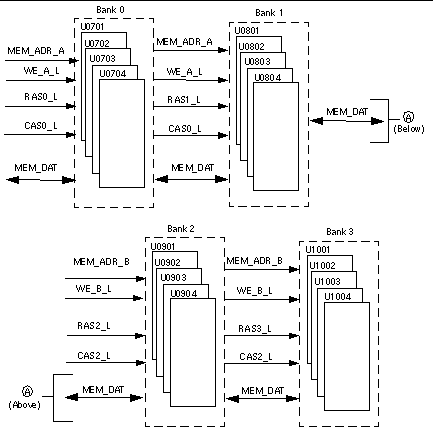
The following figure shows system memory bank locations and addresses on the main logic board.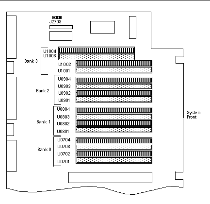
C.1.4.1 DIMM
The DIMM is a 60-nanosecond, fast-page-mode-style DIMM. Three DIMM configurations are supported in the system unit: 32-Mbyte, 64-Mbyte, and 128-Mbyte. The minimum memory capacity is 128 Mbytes (four 32-Mbyte DIMMs). The maximum memory capacity is 2 Gbytes (sixteen 128-Mbyte DIMMs).
A block of data (64 bytes) always comes from one bank of DIMMs. An error code containing the address of where a failure occurred, as well as the associated syndrome, is logged when an ECC error occurs.
There are a total of four DIMM banks in the system unit.
|
DIMM Bank |
U Number |
|
0 |
U0701 through U0704 |
|
1 |
U0801 through U0804 |
|
2 |
U0901 through U0904 |
|
3 |
U1001 through U1004 |
|
DIMM Bank |
PA[30:28] |
|
0 |
0000 |
|
|
0001 |
|
1 |
0010 |
|
|
0011 |
|
2 |
1000 |
|
|
1001 |
|
3 |
1010 |
|
|
1011 |
C.1.4.2 Memory System Timing
The QSC ASIC generates the memory addresses and control signals to the memory system. The UPA clock is the clock source for the QSC ASIC and operates as fast as 120 MHz.
C.1.5 Graphics and Imaging
The system unit takes advantage of UPA features to provide high-performance graphics capabilities. High-performance graphics can include a vertical, single-buffer UPA graphics card or a vertical, double-buffer plus Z (DBZ) UPA graphics card.
The 3DRAM is a standard dynamic random access memory (DRAM) that includes a multi-level cache and a separate graphics port. The FBC ASIC provides acceleration for 2D and 3D imaging primitives. This, combined with the 3DRAM cache and support for graphics operations, supports a high-performance frame buffer.
C.1.6 Peripherals
The following sections describe peripherals that are supported by the system:
C.1.6.1 CD-ROM Drive
The Sun StorEdgeTM CD32 CD-ROM drive is a 32x-speed (maximum) read-only random access CD-ROM device. It operates on the industry-standard SCSI-2 interface. The CD32 drive uses standard 4.76-inch (120-mm), 644-Mbyte compact disks. The Sun StorEdge CD32 Installation and User's Guide, part number 805-4237, provides cleaning, jumper setting, and operation instructions for the CD-ROM drive.
Note -
The CD-ROM drive is factory set to SCSI target ID 6. Refer to the Sun StorEdge CD32 Installation and User's Guide, part number 805-4237, to change the target address.
C.1.6.2 Hard Drives
The system supports two SCSI hard drive capacities: 9.1-Gbyte and 18-Gbyte. The hard drives have a single connector configuration. A drive bracket is used to mount the drive. The following table lists the supported hard drives.
|
Form Factor Dimension |
Disk Drive Capacity |
Wide |
RPM |
Average Seek Time (Read/Write) |
|---|---|---|---|---|
|
1.00-inch (2.54 cm) |
9.1 Gbytes |
Yes |
10K |
5.4 msec/6.2 msec |
|
1.00-inch (2.54 cm) |
18 Gbytes |
Yes |
10K |
7/5 msec/8.5 mses |
The 9-Gbyte 10K rpm Disk Drive Specifications SCA Interface, part number 805-5637, provides installation instructions, power requirements, and performance data for the 9.1-Gbyte hard drive. The 18-Gbyte 10K rpm Disk Drive Specifications, part number 806-1057, provides installation instructions, power requirements, and performance data for the 18-Gbyte 10K rpm hard drive.
C.1.7 Other RMA Storage Device X-Options
The system unit supports other removable media assembly (RMA) storage device X-options that you can install in the system unit in lieu of the CD-ROM drive. These storage device X-options include the 12-24-Gbyte 4mm DDS3 tape drive. For a listing of all X-options, refer to the product guide.
C.1.8 Keyboard and Mouse Port, and Parallel Port
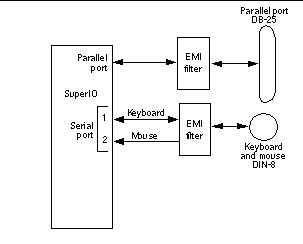
The keyboard and mouse port, as well as the parallel port interfaces are managed by the SuperIO component. For a brief description of the SuperIO, see "C.1.13 SuperIO".
C.1.8.1 Keyboard and Mouse Port
The keyboard and mouse are connected to an 8-pin DIN connector, located on the main logic board, and to two serial ports on the SuperIO component. Each serial port on the SuperIO ASIC provides 16-byte FIFO buffering. Data is asynchronously exchanged with the keyboard and mouse at 1200 baud. Keyboard current is limited to 700 milliamperes (mA) by a resettable fuse. Only the Sun Type-5 keyboard is supported.
C.1.8.2 Parallel Port
The parallel port is supported by an IEEE 1284-compatible parallel port controller that is located on the SuperIO component. The parallel port controller is a PC-industry-standard controller that achieves a 2-megabits per second (Mbps) data transfer rate. The parallel port controller interface supports the ECP protocol as well as the following:
-
Centronics - Provides a widely accepted parallel port interface.
-
Compatibility - Provides an asynchronous, byte-wide forward (host to peripheral) channel with data and status lines used according to their original definitions.
-
Nibble mode - Provides an asynchronous, reverse (peripheral-to-host) channel, under control of the host. Data bytes are transmitted as two sequential, 4-bit nibbles using four peripheral-to-host status lines.
Parallel Port Cables
The parallel port cable is IEEE1284 compliant and comprises 18 pairs of signal wires that are double shielded with braid and foil. The maximum length of the parallel port cable is 2.2 yards (2 meters).
Electrical Characteristics
Drivers operate at a nominal 5-VDC transistor-transistor logic (TTL) levels. The maximum open circuit voltage is 5.5 VDC and the minimum is -0.5 VDC. A logic high-level signal is at least 2.4 VDC at a source current of 0.32 mA and a logic low-level signal is no more than 0.4 VDC at a sink current of 14 mA.
Receivers also operate at nominal 5-VDC TTL levels and can withstand peak voltage transients between -2 VDC and 7 VDC without damage or improper operation. The high-level threshold is less than or equal to 2.0 VDC and the low-level threshold is at least 0.8 VDC. Sink current is less than or equal to 0.32 mA at 2.0 VDC and source current is less than or equal to 12 mA at 0.8 VDC.
C.1.9 Serial Port
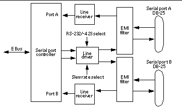
The system unit incorporates two serial ports. Each serial port is synchronous and asynchronous with full modem controls. All serial port functions are controlled by a serial port controller that is electrically connected to the system through the EBus. Line drivers and line receivers control the serial port signal levels and provide RS-232 and RS-423 compatibility. Each serial port interfaces through its own DB-25 connector.
The major features of each serial port include:
-
Two fully functional synchronous and asynchronous serial ports
-
DB-25 connectors
-
Increased baud rate speed (to 384 Kbaud, synchronous; 460.8 Kbaud, asynchronous)
-
Variable edge rate for greater performance
-
EBus interface
C.1.9.1 Serial Port Components
Serial port components include a serial port controller, line drivers, and the line receivers.
The serial port controller contains 64-byte buffers on both the input and output. This enables the serial port to require less CPU bandwidth. Interrupts are generated when the buffer reaches 32 bytes or half full. The serial port controller contains its own crystal oscillator that supports rates of up to 921.6 Kbaud.
The line drivers and line receivers are compatible with both RS-232 and RS-423. Two system board jumpers are used to set the line drivers and line receivers to either RS-232 or RS-423 protocols. The line driver slew rate is also programmable. For baud rates over 100K, the slew rate is set to 10 VDC/msec. For baud rates under 100K, the slew rate is set to 5 VDC/msec.
Serial Port Functions
The serial port provides a variety of functions. Modem connection to the serial port allows access to the internet. Synchronous X.25 modems are used for telecommunications in Europe. An ASCII text window is accessible through the serial port on non-graphic systems. Low-speed printers, button boxes (for CAD/CAM applications) and exotic devices that function like a mouse are also accessible through the serial port. The additional speed of the serial port can be used to execute communications with a CSU/DSU for a partial T1 line to the internet at 384 Kbaud per second.
EIA Levels
Each serial port supports both RS-232 and RS-423 protocols. RS-232 signaling levels are between -3 VDC and -15 VDC and +3 VDC and +15 VDC. A binary 1 (0012) is anything greater than +3 VDC and a binary 0 (0002) is anything less than -3 VDC. The signal is undefined in the transition area between -3 VDC and +3 VDC. The line driver switches at -10 VDC and +10 VDC with a maximum of -12 VDC and +12 VDC in RS-232 mode. RS-423 is similar except that signaling levels are between -4 VDC to -6 VDC and +4 VDC and +6 VDC. The line driver switches at -5.3 VDC and +5.3 VDC with a maximum of -6 V and +6 VDC. Switching from RS-232 to RS-423 protocol is accomplished by changing jumpers J2604 and J2605. Jumper positions 1 and 2 are for RS-232 and jumper positions 2 and 3 are for RS-423.
The preferred signaling protocol is RS-423. The higher voltages of R-232 make it difficult to switch at the higher baud rates. The maximum rate for RS-232 is approximately 64 Kbaud while the maximum rate for RS-423 is 460.8 Kbaud. The system default is set to RS-232.
Synchronous Rates
The serial synchronous ports operate at any rate from 50 Kbaud to 256 Kbaud when the clock is generated from the serial port controller. When the clock is generated from an external source, the synchronous ports operate at up to 384 Kbaud. Clock generation is accurate within 1 percent for any rate that is generated between 50 Kbaud and 256 Kbaud.
Asynchronous Rates
The serial asynchronous ports support twenty baud rates that are all exact divisors of the crystal frequency (with exception for 110, which is off by less than 1 percent). Baud rates include 50, 75, 110, 200, 300, 600, 1200, 1800, 2400, 4800, 9600, 19200, 38400, 57600, 76800, 115200, 153600, 230400, 307200, and 460800.
Slew Rate and Cable Length
The maximum RS-423 cable length is 118 feet (30 meters) and the maximum RS-232 cable length is 50 feet (15.24 meters). The slew rate changes depending on the speed. For speeds less than 100 Kbaud, the slew rate is set at 5 VDC per microsecond. For rates greater than 100 Kbaud, the slew rate is increased to 10 VDC per microsecond. This allows maximum performance for the greater baud rates and better signal quality at the lesser baud rates.
C.1.10 Ethernet
The system unit supports 10-Mbps, 10BASE-T, twisted-pair Ethernet and 100-Mbps, 100BASE-TX, media independent interface (MII) Ethernet with the use of a single magnetics module. Twisted-pair Ethernet is provided through an 8-pin RJ45 connector. MII Ethernet is provided through a 40-pin MII connector. The MII port allows connection to any cable medium, including unshielded twisted-pair (UTP), shielded twisted-pair (STP), and fiber optic accompanied by the appropriate external transceiver. The system automatically senses an external transceiver, thus disabling an on-board transceiver.The Ethernet circuitry design is based on a Quality Semiconductor PHY.
The PHY chip integrates a 100BASE-TX physical coding sub-layer (PCS) and a complete 10BASE-T module in a single chip. It provides a standard MII to communicate between the physical signaling and the medium access control layers for both 100BASE-TX and 10BASE-T operations. The PHY IC interfaces to the 100-Mbps physical-medium-dependent transceiver Twister IC.
The 100BASE-TX portion of the PHY IC consists of the following functional blocks:
-
Transmitter
-
Receiver
-
Clock generation module
-
Clock recovery module
The 10BASE-T section of the PHY IC consists of the 10-Mbps transceiver module with filters.
The 100BASE-TX transceiver is included in a separate Twister IC and features adaptive equalization, baseline wander correction, and transition time control on the output signals.
The 100BASE-TX and 10BASE-T sections share the following functional characteristics:
-
PCS control
-
MII registers
-
IEEE 1149.1 controller (JTAG compliance)
-
IEEE 802.3u auto negotiation
The next sections provide brief descriptions of the following:
-
Automatic negotiation
-
External transceivers
-
External cables
-
Connectors
-
MII power
-
MII port timing
C.1.10.1 Automatic Negotiation
Automatic negotiation controls the cable when a connection is established to a network device. It detects the various modes that exist in the linked partner and advertises its own abilities to automatically configure the highest performance mode of inter-operation, namely, 10BASE-T, 100BASE-TX, or 100BASE-T4 in half- and full-duplex modes.
The Ethernet port supports automatic negotiation. At power up, an on-board transceiver advertises 100BASE-TX in half-duplex mode, which is configured by the automatic negotiation to the highest common denominator based on the linked partner.
C.1.10.2 External Transceivers
The following external transceivers are connected through the MII port:
-
6211 Micro 100BASE-FX FastEthernet transceiver
-
CT4-1030 100BASE-T4 transceiver
-
CFX-107X 100BASE-FX transceiver
-
XF467A MII-to-AUI transceiver
C.1.10.3 External Cables
The MII port supports an 18 inch (0.5-meter) long, 40-conductor, 20 signal-ground, STP cable. The single-ended impedance of the cable is 68 ohms (+/-10%). The propagation delay for each twisted-pair, measured from the MII connector to the PHY, does not exceed 2.5 nanoseconds.
The RJ45 Ethernet port supports a Category 5, UTP cable for the 100BASE-TX, and a Category 3, 4, or 5 UTP cable for the 10BASE-T operation.
Note -
The maximum cable segment lengths for the 100BASE-TX and 10BASE-TX are 300 feet (100 meters) and 3000 feet (1000 meters), respectively.
C.1.10.4 Connectors
A 40-pin connector is used for the MII connector. A standard 8-pin RJ45 connector with a shield is used for the AUI connector.
C.1.10.5 MII Power
A regulated 5-VDC (+/- 5%) voltage is supplied to the PHY IC over the load range of from 0 to 750 mA. A 2-amp overcurrent protection circuit is provided by a polymer-based resettable fuse to the MII supply voltage.
MII-to-AUI connection to a 10-Mbps medium attachment unit requires a supplemental power source to meet the AUI power supply requirements. The MII-AUI converter provides the necessary supplemental power.
C.1.10.6 MII Port Timing
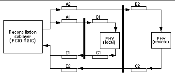
MII port timing encompasses two configurations involving the use of either an on-board transceiver or external transceivers. For either transceiver configuration, the MII port timing is the same because MII operates with a 40-nanosecond cycle time.
MII is used to interconnect both integrated circuits and circuit assemblies. This enables separate signal transmission paths to exist between the reconciliation sublayer, embedded in the PCIO ASIC, and a local PHY IC, and between the reconciliation sublayer and a remote PHY IC. The unidirectional paths between the reconciliation sublayer and the local PHY IC are composed of sections A1, B1, C1 and D1. The unidirectional paths between the reconciliation sublayer and the remote PHY IC are composed of sections A2, B2, C2, and D2.
C.1.11 SCSI
The system unit implements a small computer system interface (SCSI) Fast-20 (UltraSCSI) parallel interface bus. The UltraSCSI provides the following:
-
Efficient peer-to-peer I/O bus devices
-
Mechanical, electrical, and timing specification definition that support transfer rates of 20 or 40 Mbytes per second (corresponding to the data path width of an 8-bit, or 16-bit bus, respectively)
-
Peak bandwidth of 40 Mbytes per second (with implemented 16-bit bus width)
The internal SCSI bus is terminated at each end. One set of terminators is located close to the CD-ROM drive connector on the CD-ROM SCSI card. A second set of terminators is located close to the 68-pin external SCSI connector.

C.1.11.1 Host Adapter
The host adapter is a Symbios Logic PCI-SCSI I/O processor IC. The host adapter and all target devices comply with the Fast-20 single-ended drivers and receivers characteristics. The electrical characteristics of the output buffers include:
-
Vol (output low) equals 0 to 0.5 VDC with Iol at 48 mA (signal asserted)
-
Voh (out high) equals 2.5 to 3.7 VDC (signal negated)
-
trise (rising slew rate) equals 520 mV per nanosecond maximum (0.7 to 2.3 VDC)
-
tfall (falling slew rate) equals 520 mV per nanosecond maximum(2.3 to 0.7 VDC)
The Fast-20 electrical characteristics for the host adapter and target device include:
-
Vil (input low) equals 1.0 VDC maximum (signal true)
-
Vih (input high) equals 1.9 VDC minimum (signal false)
-
Iil (input low current) equals +/- 20 mA at Vi equals 0.5 VDC
-
Iih (input high current) equals +/- 20 mA at Vi equals 2.7 VDC
-
Minimum input hysteresis equals 0.3 VDC
C.1.11.2 Supported Target Devices
The SCSI subsystem supports a maximum of four internal devices, including the host adapter. The CD-ROM drive is a narrow device. A unipack with one drive or a six-pack, accommodating six drives, can be used as external devices.
|
Target Device |
Comment |
|---|---|
|
Internal disks |
Up to two 3.5-inch x 1.6-inch disks (9.1-Gbyte or 18-Gbyte). All internal disks are UltraSCSI-compliant. |
|
Internal CD-ROM drive |
Optional 644-Mbyte SunCD 32X speed; photo CD compatible. Headphone jack with volume control. CD-ROM drive is a narrow SCSI device. |
|
Internal tape drive(s) |
Refer to product guide. |
|
External SPARCstorage UniPack |
Refer to product guide. |
|
External SPARCstorage SixPack |
Refer to product guide. |
C.1.11.3 External Cables
External UltraSCSI-compliant SCSI cables have an impedance of 90 ohm (+/- 6 ohm) and are required for UltraSCSI interface. Sun's implementation of UltraSCSI requires that the total SCSI bus length be limited to no more than approximately 20 feet (6 meters) with up to 12 Sun compensated devices. Due to the considerably short bus length, an approximately 32-inch (0.8-meter) UltraSCSI-compliant external cable is supported (part number 530-2883) in addition to an approximate 6.5-foot (2-meter) UltraSCSI-compliant external cable (part number 530-2884).
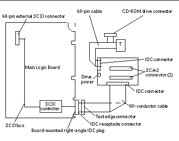
C.1.11.4 Internal SCSI Subassembly
The internal SCSI subassembly consists of two cable assemblies and two SCSI cards. The SCSI subassembly is attached to the main logic board using an insulation displacement connector (IDC) receptacle attached to a 80-conductor cable. In addition to the SCSI signals, the 80-conductor cable carries system LED signals to the SCSI backplane card. The IDC receptacle mates with a right-angle plug that is mounted on the main logic board.
The 80-conductor cable attaches on the other end to the SCSI backplane card with another IDC connector. The SCSI backplane card incorporates two SCA-2 connectors for mounting the hard drives, a four-circuit power connector to supply 5 VDC and 12 VDC power to the hard drives, and a green, right-angle LED.
A 68-conductor cable exits the SCSI backplane card, carrying 27 SCSI signals and the Termpower to the internal CD-ROM drive (or tape drive). The SCSI backplane card houses the CD-ROM drive connector and one SCSI bus terminator. The Termpower is routed through the SCSI subassembly to connect to the terminator on the SCSI backplane card in support of the multi-host configuration. The following figure shows the functionality of the internal SCSi assembly.
C.1.11.5 SCSI ID Selection
The main logic board host adapter is assigned the SCSI identification of 7 for both ports. The two internal drives attached to the SCA-2 connectors have a SCSI identification of 0 and 1, while the CD-ROM has an identification of 6.
C.1.12 ASICs
The system unit achieves a high level of integration through application-specific intergrated circuits (ASICs). All ASICs are 1149.1 (JTAG) compliant. The following ASICs are highlighted and are described in the following subsections:
-
XB9+
-
QSC
-
PCI-to EBus/Ethernet controller (PCIO)
-
UPA-to-PCI bridge (U2P)
-
Frame buffer controller (FBC)
-
Reset, interrupt, scan, and clock (RISC)
C.1.12.1 XB9+
The XB9+ ASIC is a buffered memory crossbar device that acts as the bridge between the six system unit buses. The six system unit buses include two processor buses, a memory data bus, a graphics bus, and two I/O buses. The XB9+ ASIC provides the following:
-
Six-port crossbar
-
Decoupled memory port; loading and unloading of memory data can take place in parallel with other operations
-
Burst transfers operate on a doubleword of data per slice
-
A total of eight two-entry first-in-first-out (FIFO) devices for read data storage
-
Power-up safe buses (tristated)
C.1.12.2 QSC
The QSC ASIC provides system control. It controls the UPA interconnect between the major system unit components and main memory. The QSC ASIC provides the following:
-
Interconnect packet receive
-
Memory arbiter
-
Non-cached arbiter
-
Memory controller
-
Snoop interface
-
Coherence controller
-
S_register dispatcher
-
Internet packet send
-
Datapatch scheduler
-
EBus interface
C.1.12.3 PCIO
The PCI-to-EBus/Ethernet controller (PCIO) ASIC performs dual roles: PCI bus-to-Ebus bridging and Ethernet control. The PCIO ASIC provides the electrical connection between the PCI bus and all other I/O functions. In addition, the PCIO ASIC contains an embedded Ethernet controller to manage Ethernet transactions and provides the electrical connection to slower on-board functions, such as the flash PROM and the audio module.
C.1.12.4 U2P
The UPA-to-PCI bridge (U2P) ASIC provides an I/O connection between the UPA bus and the two PCI buses. The U2P ASIC features include:
-
Full master and slave port connection to the high-speed UPA interconnect. The UPA is a split address/data packet-switched bus that has a potential data throughput rate of greater than 1 Gbyte per second. UPA data is ECC protected.
-
Two physically separate PCI bus segments with full master and slave support:
-
66-MHz PCI bus segment (PCI bus A): 3.3-VDC I/O signaling, 64-bit data bus, compatible with the PCI 66-MHz extensions, support for up to four master devices (at 33 MHz only)
-
33-MHz PCI bus segment (PCI bus B): 5.0-VDC I/O signaling, 64-bit data bus, support for up to six master devices
-
Two separate 16-entry streaming caches, one for each bus segment, for accelerating some kinds of PCI DVMA activity. Single IOMMU with 16-entry TLB for mapping DVMA addresses for both buses (IOMMU used to translate 32-bit or 64-bit PCI addresses into 41-bit UPA addresses).
-
A mondo-vector dispatch unit for delivering interrupt requests to CPU modules, including support for PCI interrupts from up to six slots, as well as interrupts from on-board I/O devices.
C.1.12.5 FBC
The frame buffer controller (FBC) ASIC is the graphics draw ASIC that provides interface between the UPA and the 3DRAM. The FBC ASIC provides 2D and 3D graphics draw acceleration. Highlights of the FBC ASIC features include:
-
UPA slave device with write-mostly philosophy
-
Interfaces with 3DRAM to achieve accelerated graphics performance
-
Supports single buffered and DBZ configurations
-
Supports frame buffer-to-frame buffer copy
-
Supports viewport clipping, picking, and pixel processing
-
Supports byte, plane masks, raster operations, blend operations, and conditional writes in 3DRAM
-
83.3-MHz UPA operation and 75-MHz 3DRAM operation
-
3.3-VDC and 5-VDC (for RAMDAC ASIC) supply voltage
C.1.12.6 RISC
The reset, interrupt, scan, and clock (RISC) ASIC implements four functions: reset, interrupt, scan, and clock. Generation and stretching of the reset pulse is performed in this ASIC. Interrupt logic concentrates 42 different interrupt sources into a 6-bit code, which communicates with the U2P ASIC. It also integrates a JTAG controller.
Highlights of the RISC ASIC features include:
-
Determines system clock frequency
-
Controls reset generation
-
Performs PCI bus and miscellaneous interrupt concentration for U2P
-
Controls flash PROM programming, frequency margining, and lab console operation
-
33-MHz operation
-
3.3-VDC and 5-VDC supply voltage
C.1.13 SuperIO
The SuperIO is a commercial, off-the-shelf component that controls the keyboard, diskette, and parallel port interfaces. It contains a DMA-driven diskette controller, two serial port controllers, an IEEE 1284 parallel port interface, and an IDE disk interface (not currently used). The SuperIO drives the various ports directly with some EMI filtering on the keyboard and parallel port signals. Support for mixed voltage modes and power management features for low power operation are also included. Features of the SuperIO include:
-
Two independent serial ports used for keyboard and mouse
-
N82077 diskette drive interface
-
IEEE 1284 parallel port interface
C.1.14 Power Supply
The system unit uses a 380-watt power supply that operates under the voltage range of 90 to 264 volts root-mean-square (Vrms) and a frequency range of 47 to 63 Hz. The maximum input current is 6.3.
The power supply continues to regulate all outputs for 20 milliseconds after AC power is removed.
|
Output |
Voltage (VDC) |
Maximum Current (A) |
Regulation Band |
|---|---|---|---|
|
1 |
3.3 |
50.0 |
3.23 to 3.43 |
|
2 |
5.0 |
40.0 |
4.95 to 5.15 |
|
3 |
12.0 |
5.0 |
11.40 to 12.60 |
|
4 |
-12.0 |
0.5 |
-12.60 to -11.40 |
|
5 |
5.1 |
1.0 |
4.95-5.25 |
Note -
The combined power of output 1 and output 3 must be less than 320 watts.
C.1.15 Control Signals
With the exception of the PowerOn signal, all power supply control signals are at TTL signal levels.
|
Parameter |
Minimum |
Maximum |
|---|---|---|
|
VOH (high-level output voltage) |
2.4 VDC |
|
|
VOL (low-level output voltage) |
|
0.4 VDC |
|
VIH (high-level input voltage) |
2.0 VDC |
|
|
VIL (low-level input voltage) |
|
0.8 VDC |
C.1.15.1 Remote Enable PowerOn
A remote interface can enable the DC outputs with a low signal to the PowerOn input and the DC outputs with a high signal to the PowerOn input. The signal is interfaced to the power supply through the main logic board and the power distribution board.
C.1.15.2 System Unit Power Budget
The following subsections present the system unit power budgets.
PCI Cards
The PCI card power budget supports a total of 60 watts, which is distributed among four PCI cards in an arbitrary way as long as the total PCI power does not exceed 60 watts.
The following table lists 5 VDC PCI card power estimates
|
Voltage Rail (VDC) |
PCI Cards (Maximum Number) |
Current Each (Amps) |
Current Total (Amps) |
Total Power (Watts) |
|---|---|---|---|---|
|
5 |
4 |
3.0 |
12.0 |
<= 60 for all voltage rails combined |
|
3.3 |
0 |
0 |
0 |
|
|
+12 |
4 |
0.4 |
1.6 |
|
|
-12 |
4 |
0.1 |
0.4 |
.
The following table lists 3.3VDC PCI card power estimates.
|
Voltage Rail (VDC) |
PCI Cards (Maximum Number) |
Current Each (Amps) |
Current Total (Amps) |
Total Power (Watts) |
|---|---|---|---|---|
|
5 |
0 |
0 |
0 |
<= 60 for all voltage rails combined |
|
3.3 |
4 |
4.5 |
18.0 |
|
|
+12 |
4 |
0.4 |
1.6 |
|
|
-12 |
4 |
0.1 |
0.4 |
Memory System
The following table lists the memory system power budget.
|
Number of DIMMs |
WC Current Total (Amps) |
Total Power @5 VDC (Watts) |
|---|---|---|
|
16 |
9.33 |
46.66 |
C.1.16 Standard System Facilities
In addition to the previously listed features, the system unit provides the following:
-
TOD/NVRAM for clock and identification functions
-
Flash PROM for operating system initialization. The flash PROM is re-programmable through UNIX and OBP utilities.
C.1.17 Main Logic Board
The following figure illustrates a block diagram of the system's main logic board.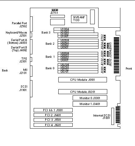
- © 2010, Oracle Corporation and/or its affiliates
