This appendix contains information about the following connector pinouts:
C.1 3-Cable Dongle Pinouts
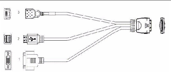
The following figure and table provides pinout information for the 3-cable dongle connectors.
FIGURE C-1 3-Cable Dongle Connectors (P/N 530-3936 Option # 4622A)

Figure Legend Pinouts for 3-Cable Dongle Connectors (Option# 4622A)
|
3
RJ-45
|
RJ-45 Serial Signal
|
2
USB
|
USB Signal
|
1
VGA
|
VGA Signal
|
|
1
|
RTS
|
1
|
USB1 VCC
|
1
|
Red
|
|
2
|
DTR
|
2
|
USB1 DN
|
2
|
Green
|
|
3
|
Trasnmit Data
|
3
|
USB1 DP
|
3
|
Blue
|
|
4
|
Ground
|
4
|
USB1 Ground
|
4
|
Not used
|
|
5
|
Ground
|
5
|
USB2 Ground
|
5
|
Ground
|
|
6
|
Recive Data
|
6
|
USB2 DP
|
6
|
Ground
|
|
7
|
DSR and DCD
|
7
|
USB2 DP
|
7
|
Ground
|
|
8
|
CTS
|
8
|
USB2 Ground
|
8
|
Ground
|
|
9
|
5V
|
|
10
|
Ground
|
|
11
|
Ground
|
|
12
|
VGA Data
|
|
13
|
H_Sync
|
|
14
|
V_Sync
|
C.2 4-Cable Dongle Pinouts
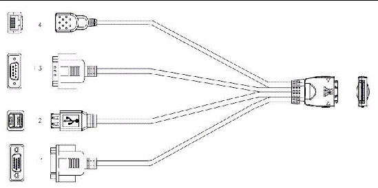
The following figure and table provides pinout information for the 4-cable dongle connectors.
FIGURE C-2 4-Cable Dongle Connectors (P/N 530-3934 Option # 4621A)

Figure Legend Pinouts for 4-Cable Dongle Connectors (Option# 4622A)
|
4
RJ-45
|
RJ-45 Signal
|
3
Serial
|
Serial Signal
|
2
USB
|
USB Signal
|
1‘
VGA
|
VGA Signal
|
|
Note - The RJ-45 serial connector on the 4-Cable Dongle (Option# 4621A) is not functional on the Sun Blade Sun Blade X6270 Server Module.
|
1
|
DCD
|
1
|
USB1 VCC
|
1
|
Red
|
|
2
|
Receive Data
|
2
|
USB1 DN
|
2
|
Green
|
|
3
|
Trasnmit Data
|
3
|
USB1 DP
|
3
|
Blue
|
|
4
|
DTR
|
4
|
USB1 Ground
|
4
|
Not used
|
|
5
|
Ground
|
5
|
USB2 VCC
|
5
|
Ground
|
|
6
|
DSR
|
6
|
USB2 DN
|
6
|
Ground
|
|
7
|
RTS
|
7
|
USB2 DP
|
7
|
Ground
|
|
8
|
CTS
|
8
|
USB2 Ground
|
8
|
Ground
|
|
9
|
RI
|
9
|
5V
|
|
|
|
10
|
Ground
|
|
|
|
11
|
Ground
|
|
|
|
12
|
Data
|
|
|
|
13
|
H_Sync
|
|
|
|
14
|
V_Sync
|
|
|
|
|
|
15
|
Clock
|
C.3 SAS/SATA Connectors
The Serial Attached SCSI (SAS)/Serial Advanced Technology Attachment (SATA) connector pins and their corresponding descriptions are shown in the figure and table in this section.
FIGURE C-3 SAS/SATA Connector

TABLE C-1 SAS/SATA Connector Pins
|
Segment
|
Pin Number
|
Pin Name
|
Description
|
|
Signal Segment
|
S1
|
Gnd
|
Second mate ground
|
|
S2
|
TX+
|
Positive side of transmit to hard drive
|
|
S3
|
TX-
|
Negative side of transmit to hard drive
|
|
S4
|
Gnd
|
Second mate ground
|
|
S5
|
RX-
|
Negative side of receive from hard drive
|
|
S6
|
RX+
|
Positive side of receive from hard drive
|
|
S7
|
Gnd
|
Second mate ground
|
|
Backside Signal Segment
|
S8
|
Gnd
|
Second mate ground
|
|
S9
|
|
Not used
|
|
S10
|
|
Not used
|
|
S11
|
Gnd
|
Second mate ground
|
|
S12
|
|
Not used
|
|
S13
|
|
Not used
|
|
S14
|
Gnd
|
Second mate ground
|
|
Power Segment
|
P1
|
3.3 V
|
Not used
|
|
P2
|
3.3 V
|
Not used
|
|
P3
|
3.3 V
|
Not used
|
|
P4
|
Gnd
|
First mate ground
|
|
P5
|
Gnd
|
Second mate ground
|
|
P6
|
Gnd
|
Second mate ground
|
|
P7
|
5.0 V
|
Pre-charge, second mate
|
|
P8
|
5.0 V
|
|
|
P9
|
5.0 V
|
|
|
P10
|
Gnd
|
Second mate ground
|
|
P11
|
Reserved
|
Should be grounded
|
|
P12
|
Gnd
|
First mate ground
|
|
P13
|
12.0 V
|
Pre-charge, second mate
|
|
P14
|
12.0 V
|
|
|
P15
|
12.0 V
|
|
C.4 SAS Diskplane
The SAS diskplane connector pins and their corresponding descriptions are shown in the following table.
TABLE C-2 SAS Disk Backplane Signal Connector Pins
|
Pin Number
|
Signal Name
|
|
1, 4, 7
|
GND
|
|
2, 3
|
TX+/TX-
|
|
5, 6
|
RX+/RX-
|
C.5 SAS Power/LED Connector
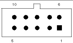
The SAS power/LED connector pins and their corresponding descriptions are shown in the figure and table in this section.
FIGURE C-4 SAS Power/LED Connector

TABLE C-3 SAS Power/LED Connector Pins
|
Pin Number
|
Signal Name
|
|
1
|
DISK1_FAULT_LED_L
|
|
2
|
DISK1_RDY2RM_L
|
|
3
|
DISK1_PRSNT_L
|
|
4
|
12V
|
|
5
|
GND
|
|
6
|
DISK0_FAULT_LED_L
|
|
7
|
DISK0_RDY2RM_L
|
|
8
|
DISK0_PRSNT_L
|
|
9
|
GND
|
|
10
|
5V
|
C.6 Compact Flash
The Compact Flash connector pins and their corresponding descriptions are shown in the figure and table in this section.
FIGURE C-5 Compact Flash Connector

TABLE C-4 Compact Flash Connector Pins
|
Signal Name
|
Pin #
|
Pin #
|
Signal Name
|
|
GND
|
1
|
26
|
PRSNT_N
|
|
D03
|
2
|
27
|
D11
|
|
D04
|
3
|
28
|
D12
|
|
D05
|
4
|
29
|
D13
|
|
D06
|
5
|
30
|
D14
|
|
D07
|
6
|
31
|
D15
|
|
CS1_L
|
7
|
32
|
CS3_L
|
|
GND
|
8
|
33
|
No Connect
|
|
ATA_SEL
|
9
|
34
|
IOR_L
|
|
GND
|
10
|
35
|
IOW_L
|
|
GND
|
11
|
36
|
WE
|
|
GND
|
12
|
37
|
INT_L
|
|
3.3V
|
13
|
38
|
3.3V
|
|
GND
|
14
|
39
|
IDE_CSEL
|
|
GND
|
15
|
40
|
No Connect
|
|
GND
|
16
|
41
|
IDE_RESET_L
|
|
GND
|
17
|
42
|
IDE_RDY
|
|
ADDR2
|
18
|
43
|
DRQ_L
|
|
ADDR1
|
19
|
44
|
DACK_L
|
|
ADDR0
|
20
|
45
|
No Connect
|
|
D00
|
21
|
46
|
No Connect
|
|
D01
|
22
|
47
|
D08
|
|
D02
|
23
|
48
|
D09
|
|
No Connect
|
24
|
47
|
D10
|
|
IDE_CD2
|
15
|
50
|
GND
|
| Sun Blade X6270 Server Module Service Manual
|
820-6178-13
|
    |
Copyright © 2010, Oracle and/or its affiliates. All rights reserved.
