
Table B-1 describes card cage slot assignments for printed circuit boards in SPARCsystem 670MP.
Note -
For slot assignment information of other 12-slot systems, refer to
o SPARCsystem 470 Card Cage Slot Assignment and Back Plane Configuration
o SPARCsystem 370 Card Cage Slot Assignment and Back Plane Configuration
o Sun Systems Card Cage Slot Assignment and Back Plane Configuration
The table vertically lists PCB slot priority assignments in order of descending priority. Horizontal slot designations "A", "B", "C", etc., correspond to preferred locations for the specific board, with "A" being the most desirable location. If the only designation is "A", the board MUST be placed in that slot. Boards must be installed in descending order starting with the system board.
Note - If the boards are not installed in the proper order, the system may lose performance or functionality.
Note - Slots 1 through 3 are non- VME slots; reserved for memory boards only.
Figure B-1 shows SPARCsystem 670MP back plane slot numbering and bus locations. Figure B-2 shows back plane jumper layout. Table B-2 and Table B-2 further describe back plane jumper locations and functions.
-------------------------------------------------------------------------------------------------------------------------------------------------------------------------------------------------------------------


Back Plane          Board Name                                         Back Plane Slot Position
Jumpers
-------------------------------------------------------------------------------------------------------------------------------------------------------------------------------------------------------------------


BG3          IACK                                                      1                         2      3  4      5  6                            7                 8                       9             10         11      12
PX03         PX04
-------------------------------------------------------------------------------------------------------------------------------------------------------------------------------------------------------------------
(a)          (a)    600MP System Board (a)                                                                 A  A

N/A          N/A    1st Memory Board (b)                                                         A  A

IN           IN     2nd Memory Board (b)                                                                             A  A

IN           IN     1st SBus Expansion Subsystem (j)                                             A  A                A   A   -  -  -  -  -  -  -  -  -  -  A   A

IN           IN     2nd SBus Expansion Subsystem (j)                                                                                                                B   B   -  -  -  -  -  B   B

OUT          OUT    1st 501-1460 SunLink Channel Adapter (d,e)                                                       A   A   -  -  -  -  -  -  -  -  -  -  A   A

OUT          OUT    2nd 501-1460 SunLink Channel Adapter (d,e)                                                                                                      B   B   -  -  -  -  -  B   B

OUT          OUT    1st 501-1276 Fiber Distributed Data Interface (f)                                                A  -  -  -  -  -  -  -  -  -  -  -  A

OUT          OUT    2nd 501-1276 Fiber Distributed Data Interface (f)                                                                             B  -  -  -  -  -  -  -  -  -  B

IN           IN     501-1847 Prestoserve (g)                                                                                                                        A  -  -  -  -  -  -  -  A

OUT          OUT    1st 370-1421 Sun VME Network CoProcessor (k)                                                     A  -  -  -  -  -  -  -  -  -  -  -  A

OUT          OUT    2nd 370-1421 Sun VME Network CoProcessor (k)                                                                                  B  -  -  -  -  -  -  -  -  -  B

OUT          OUT    3rd 370-1421 Sun VME Network CoProcessor (k)                                                                                                    C -  -  -  -  -  -  -   C

OUT          OUT    4th 370-1421 Sun VME Network CoProcessor (k)                                                                                                                            D  -  -  -  -  -  D

OUT          OUT    1st ISP-80 Controller (h, i)                                                                     A  -  -  -  -  -  -  -  -  -  -  -  A

OUT          OUT    2nd ISP-80 Controller (h, i)                                                                                                  B  -  -  -  -  -  -  -  -  -  B

OUT          OUT    3nd ISP-80 Controller (h, i)                                                                                                                    C -  -  -  -  -  -  -   C

OUT          OUT    4th ISP-80 Controller (h, i)                                                                                                                                            D  -  -  -  -  -  D

IN           OUT    1st 501-1221 MCP (c,e)                                                                                                        A   -  -  -  -  -  -  -  -  -  A

IN           OUT    2nd 501-1221 MCP (c,e)                                                                                                                          B  -  -  -  -  -  -  -   B

IN           OUT    3rd 501-1221 MCP (c,e)                                                                                                                                                  C ` -  -  -  -  -   C

IN           OUT    4th 501-1221 MCP (c,e)                                                                                                                                                                D  -  -  -   D

IN           OUT    1st 501-1203 ALM-2 (c)                                                                                                        A  -  -  -  -  -  -  -  -  -  A

IN           OUT    2nd 501-1203 ALM-2 (c)                                                                                                                          B -  -  -  -  -  -  -   B

IN           OUT    3rd 501-1203 ALM-2 (c)                                                                                                                                                  C -  -  -  -  -   C

IN           OUT    4th 501-1203 ALM-2 (c)                                                                                                                                                                D  -  -  -   D

IN           OUT    5th 501-1203 ALM-2 (c)                                                                                                                                                                           E  -  E

IN           OUT    6th 501-1203 ALM-2 (c)                                                                                                                                                                                   F

-------------------------------------------------------------------------------------------------------------------------------------------------------------------------------------------------------------------
These notes refer to parenthesized letters, such as (a) or (b), in Table B-1.
See Table B-2. Each jumper listed (left column) connects
P1_BG0IN*-P1_BG3IN* to P1_BG0OUT*-P1_BG3OUT* and IACKIN* to P!_IACKOUT* on the card cage slot (right column).
Table B-2 shows jumper location on the back plane for each jumper function. Bus termination is provided by the Clock jumpers which must be IN at locations P10, P11, P12, and P13. The +5v standby jumper must be in at P100.
-------------


Jumper  Slot
-------------
P4XX    4

P5XX    5

P6XX    6

P7XX    7

P8XX    8

P9XX    9

P10XX   10

P11XX   11

P12XX   12

-------------
---------------------------------


Jumper Function  Jumper Location
---------------------------------
BG0              PX00

BG1              PX01

BG2              PX02

BG3              PX03

BG4              PX04

+5V STBY         P100

CLOCK            P10

                 P11

                 P12

                 P13

---------------------------------
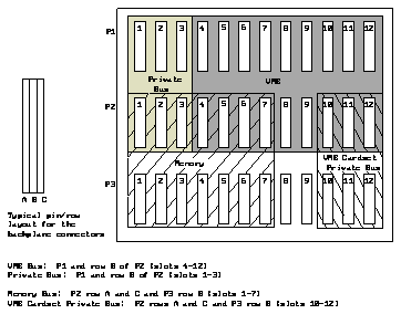
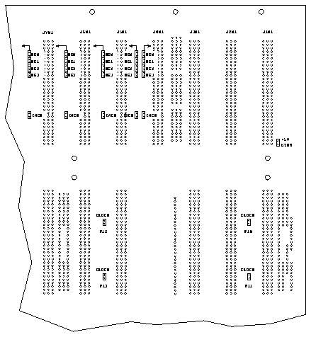
Figure B-2 SPARCsystem 670MP Back Plane Jumpers
Six VME based communication boards total (MCP and ALM-2) may reside in the system at one time. Any combination of up to four MCP and six ALM-2 options maybe configured for this system.
The Asynchronous Line Multiplexer-2 (ALM-2) shares VME interrupt vector
assignments and address space with the Multiprotocol Communication
Processor (MCP). Because of these possible conflicts, and a possible physical
space restriction in the Data Center Cabinet, the following must be applied
when installing an ALM-2 into a card cage that also contains MCPs.
-------------------------------------------------------------------------------


Installed Board           Device Address (Hex)  VME Vector Interrupt Assignment
-------------------------------------------------------------------------------
1st Board (ALM-2 or MCP)  0x01000000            8b

2nd Board (ALM-2 or MCP)  0x01010000            8a

3rd Board (ALM-2 or MCP)  0x01020000            89

4th Board (ALM-2 or MCP)  0x01030000            88

5th Board (ALM-2)         0x02000000            a0

6th Board (ALM-2)         0x02010000            a1

-------------------------------------------------------------------------------
As you can see from the table, the vector interrupt assignments of the ALM-2 and the MCP are the same. This makes the following instructions necessary.
When installing ALM-2 or MCP, you must install them in proper address order. Four VME board address positions exist to accommodate the ALM-2 or MCP board (devices 0-3). Thus, a given address position can accommodate one board type only. MCP or ALM-2 must be installed in proper device sequence.
Table B-5 Board Device Sequence
-----------------------------------


1st Board (ALM-2 or MCP)  Device 0

2nd Board (ALM-2 or MCP)  Device 1

3rd Board (ALM-2 or MCP)  Device 2

4th Board (ALM-2 or MCP)  Device 3

5th Board (ALM-2)         Device 4

6th Board (ALM-2)         Device 5

-----------------------------------
Note - Refer to the specific ALM-2 or MCP Configuration Procedure for information on board device addressing
For example, if two MCP boards are installed (1st and 2nd MCP boards) and you then wanted to install two ALM-2 boards, you would configure and install the two ALM-2 boards as 3rd and 4th ALM-2 boards respectively.
Do not install ALM-2 and MCP using identical VME addresses (board device numbers).
The ALM-2 board number (VME Address) is hardware selected on the board. If necessary, refer to the ALM-2 Installation and Configuration Manual, PN 813-1029 for information on setting/verifying ALM-2 board address (board address selection is identical for the MCP).
ALM-2 and MCP boards occupy identical VME address space and interrupt vectors, and both are known to the system board as mcpx (where x is a number 0 through 5). For example, if two MCP boards are present in the card cage and you wish to add ALM-2, the ALM-2 is designated as mcp2 in VME addressing (with two MCP boards being designated mcp0 and mcp1 respectively).