Connector Pinouts and Switch Settings
|
This appendix describes the Netra CP2140 board connector pinouts and switch settings.
A.1 CompactPCI Connectors
TABLE A-1 through contain the pinouts of the CompactPCI connectors. The J1 and J2 connector pinouts follow the CompactPCI specification. The J3, J4, and J5 connectors contain semi-custom pinouts.
FIGURE A-1 shows the Netra CP2140 board connectors.
FIGURE A-1 Netra CP2140 Board Connectors
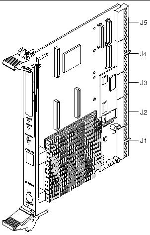
FIGURE A-2 shows the J1 connector.
FIGURE A-2 J1 Connector
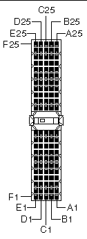
TABLE A-1 shows the J1/P1 connector pin assignments
TABLE A-1 J1/P1 Connector Pin Assignments
|
Pin #
|
Row Z
|
Row A
|
Row B
|
Row C
|
Row D
|
Row E
|
Row F
|
|
25
|
GND
|
+5V
|
REQ64#
|
ENUM#
|
+3.3V
|
+5V
|
GND
|
|
24
|
GND
|
AD[1]
|
+5V
|
+5Va
|
AD[0]
|
ACK64#
|
GND
|
|
23
|
GND
|
+3.3V
|
AD[4]
|
AD[3]
|
+5V
|
AD[2]
|
GND
|
|
22
|
GND
|
AD[7]
|
GND
|
+3.3V
|
AD[6]
|
AD[5]
|
GND
|
|
21
|
GND
|
+3.3V
|
AD[9]
|
AD[8]
|
M66EN
|
C/BE[0]#
|
GND
|
|
20
|
GND
|
AD[12]
|
GND
|
+5Va
|
AD[11]
|
AD[10]
|
GND
|
|
19
|
GND
|
+3.3V
|
AD[15]
|
AD[14]
|
GND
|
AD[13]
|
GND
|
|
18
|
GND
|
SERR#
|
GND
|
+3.3V
|
PAR
|
C/BE[1]#
|
GND
|
|
17
|
GND
|
+3.3V
|
IPMB SCL
|
IPMB SDA
|
GND
|
PERR#
|
GND
|
|
16
|
GND
|
DEVSEL#
|
GND
|
+5Va
|
STOP#
|
LOCK#
|
GND
|
|
15
|
GND
|
+3.3V
|
FRAME#
|
IRDY#
|
BD_SEL
|
TRDY#
|
GND
|
|
14
|
Key
|
|
|
|
|
|
Key
|
|
13
|
Key
|
|
|
|
|
|
Key
|
|
12
|
Key
|
|
|
|
|
|
Key
|
|
11
|
GND
|
AD[18]
|
AD[17]
|
AD[16]
|
GND
|
C/BE[2]#
|
GND
|
|
10
|
GND
|
AD[21]
|
GND
|
+3.3V
|
AD[20]
|
AD[19]
|
GND
|
|
9
|
GND
|
C/BE[3]#
|
IDSEL
|
AD[23]
|
GND
|
AD[22]
|
GND
|
|
8
|
GND
|
AD[26]
|
GND
|
+5Va
|
AD[25]
|
AD[24]
|
GND
|
|
7
|
GND
|
AD[30]
|
AD[29]
|
AD[28]
|
GND
|
AD[27]
|
GND
|
|
6
|
GND
|
REQ0#
|
GND
|
+3.3V
|
CLK0
|
AD[31]
|
GND
|
|
5
|
GND
|
BRSVP
|
BRSVP
|
RST#
|
GND
|
GNT0#
|
GND
|
|
4
|
GND
|
IPMB_PWR
|
HEALTHY_out
|
+5Va
|
intp
|
ints
|
GND
|
|
3
|
GND
|
INTA#
|
INTB#
|
INTC#
|
+5V
|
INTD#
|
GND
|
|
2
|
GND
|
tck
|
+5V
|
tms
|
tdo
|
tdi
|
GND
|
|
1
|
GND
|
+5V
|
-12V
|
trst
|
+12V
|
+5V
|
GND
|
TABLE A-2 Signal Definitions
|
AD[0..63]:
|
cPCI interface 64-bit multiplexed address and data bus
|
|
INT[A-D]:
|
cPCI interface interrupt requests
|
|
REQ64#:
|
cPCI interface request 64-bit transfer
|
|
ENUM#:
|
PICMG 2.1 R1.0 Hot-swap signal - provided to inform System Host that a board has been freshly inserted or is about to be extracted
|
|
ACK64#:
|
cPCI interface 64-bit acknowledge transfer
|
|
M66EN#:
|
Routed to IChip2, 66MHz enable - not supported
|
|
SERR#:
|
cPCI interface System Error for reporting address/data parity errors on the special cycle command
|
|
PAR:
|
cPCI interface even Parity across AD[31..0] and C/BE[3..0]
|
|
C/BE[0..7]#:
|
cPCI Bus Command and Byte Enables multiplexed on the same PCI pins
|
|
IPMB_SCL:
|
Independent Platform Management Bus Clock - see cPCI System Management Specification PICMG 2.9 R1.0
|
|
IPMB_SDA:
|
Independent Platform Management Bus Data - see cPCI System Management Specification PICMG 2.9 R1.0
|
|
PERR#:
|
Parity Error used for reporting of data parity errors
|
|
DEVSEL#:
|
cPCI interface signal Device Select.
|
|
STOP#:
|
cPCI interface signal indicates the current device is requesting the master to stop the current transaction
|
|
LOCK#:
|
cPCI interface signal indicates an operation to a bridge that may require multiple transactions to complete - not supported
|
|
FRAME#:
|
cPCI interface signal indicates the beginning and duration of an access
|
|
IRDY#:
|
cPCI interface signal - Initiator Ready indicate s the bus master s ability to complete the current data phase of the transaction
|
|
BD_SEL#:
|
PICMG 2.1 R1.0 Hot-swap signal - pulled up on the CP2140 unit and driven low to enable power on
|
|
TRDY#:
|
cPCI interface signal Target Ready indicates the selected device s ability to complete the current data phase of the transaction
|
|
IDSEL:
|
cPCI interface signal - Initialization Device Select used as a chip select during read and write transactions
|
|
REQ[0..7]#:
|
cPCI interface signal - request indicates to the arbiter that an agent desires use of the cPCI bus.
|
|
GNT[0..7]#:
|
cPCI interface signal - grant indicates to the agent that the access to the bus has been granted.
|
|
CLK[0..7]:
|
Driven by the SBC - provides timing for all transactions
|
|
IPMB_PWR:
|
Battery back-up power - see CompactPCI System Management Specification PICMG 2.9 R1.0
|
|
HEALTHY_OUT:
|
Radial signal used to acknowledge the health of the board -signals that the board is suitable to be released form reset and allowed onto the bus - see PICMG 2.1 R1.0 Hot-swap Specification.
|
|
INTP:
|
Non-cPCI interrupt, legacy IDE - not supported, 1Kohm pullup provided
|
|
INTS:
|
Non-cPCI interrupt legacy IDE - not supported
|
|
TCK, TMS, TDO, TDI:
|
JTAG signals, not supported - unconnected.
|
FIGURE A-3 Netra CP2140 Board J2 Connector

See for J2/P2 connector pin assignments.
TABLE A-3 J2/P2 Connector Pin Assignments
|
Pin #
|
Row Z
|
Row A
|
Row B
|
Row C
|
Row D
|
Row E
|
Row F
|
|
22
|
GND
|
GA4
|
GA3
|
GA2
|
GA1
|
GA0
|
GND
|
|
21
|
GND
|
CLK6
|
GND
|
BRSVP
|
BRSVP
|
BD_OFF_OUT
|
GND
|
|
20
|
GND
|
CLK5
|
GND
|
ALTSYSEN_L
|
GND
|
BD_OFF_IN
|
GND
|
|
19
|
GND
|
GND
|
GND
|
I2C_SDA
|
I2C_SCK
|
ALERT
|
GND
|
|
18
|
GND
|
BRSVP
|
BRSVP
|
BRSVP
|
GND
|
BRSVP
|
GND
|
|
17
|
GND
|
BRSVP
|
GND
|
PRST#
|
REQ6#
|
GNT6#
|
GND
|
|
16
|
GND
|
BRSVP
|
BRSVP
|
DEG#
|
GND
|
BRSVP
|
GND
|
|
15
|
GND
|
BRSVP
|
GND
|
FAL#
|
REQ5#
|
GNT5#
|
GND
|
|
14
|
GND
|
AD[35]
|
AD[34]
|
AD[33]
|
GND
|
AD[32]
|
GND
|
|
13
|
GND
|
AD[38]
|
GND
|
+5Va
|
AD[37]
|
AD[36]
|
GND
|
|
12
|
GND
|
AD[42]
|
AD[41]
|
AD[40]
|
GND
|
AD[39]
|
GND
|
|
11
|
GND
|
AD[45]
|
GND
|
+5Va
|
AD[44]
|
AD[43]
|
GND
|
|
10
|
GND
|
AD[49]
|
AD[48]
|
AD[47]
|
GND
|
AD[46]
|
GND
|
|
9
|
GND
|
AD[52]
|
GND
|
+5Va
|
AD[51]
|
AD[50]
|
GND
|
|
8
|
GND
|
AD[56]
|
AD[55]
|
AD[54]
|
GND
|
AD[53]
|
GND
|
|
7
|
GND
|
AD[59]
|
GND
|
+5Va
|
AD[58]
|
AD[57]
|
GND
|
|
6
|
GND
|
AD[63]
|
AD[62]
|
AD[61]
|
GND
|
AD[60]
|
GND
|
|
5
|
GND
|
C/BE[5]#
|
64_EN_L
|
+5Va
|
C/BE[4]#
|
PAR64
|
GND
|
|
4
|
GND
|
RSS_L
|
BRSVP
|
C/BE[7]#
|
GND
|
C/BE[6]#
|
GND
|
|
3
|
GND
|
CLK4
|
GND
|
GNT3#
|
REQ4#
|
GNT4#
|
GND
|
|
2
|
GND
|
CLK2
|
CLK3
|
SYSEN#
|
GNT2#
|
REQ3#
|
GND
|
|
1
|
GND
|
CLK1
|
GND
|
REQ1#
|
GNT1#
|
REQ2#
|
GND
|
TABLE A-4 Signal Definitions
|
GA[0..4]:
|
Geographical Addressing signals for unique slot identification
|
|
BRSVP:
|
Reserve pins - leave unconnected on backplane
|
|
BD_OFF_OUT:
|
Pulse Reset out used for dual host failover - dual host function not supported, leave unconnected on backplane
|
|
ALTSYSEN_L:
|
PICMG Redundant System Slot Spec 2.13 - Alternate System Controller Enable signal - dual host function not supported, leave unconnected on backplane
|
|
BD_OFF_IN:
|
Pulse Reset in used for dual host failover - dual host function not supported, leave unconnected on backplane
|
|
I2C_SDA:
|
In a dual host system, Inter-Host I2C Bus Data - dual host function not supported, leave unconnected on backplane
|
|
I2C_SCK:
|
In a dual host system, Inter-Host I2C Bus Clock - dual host function not supported, leave unconnected on backplane
|
|
ALERT:
|
cPCI System Management Specification PICMG 2.9 R1.0 signal input to the SMC
|
|
PRST#:
|
Backplane Push Button Reset input to the SMC
|
|
DEG#, FAL#:
|
Power Subsystem status signals input to the SMC
|
|
64_EN_L:
|
PICMG Hot-swap Spec 2.1 R1.0 signal - used to designate 64-bit capability for the slot into which the board is plugged
|
|
PAR64:
|
cPCI interface signal even parity bit that protects AD[32..63] and C/ BE[7..4]#
|
|
SYSEN#:
|
System Slot identification, grounded on the cPCI slot so the board can identify installation into the system slot.
|
|
RSS#:
|
PICMG Redundant System Slot Spec 2.13 - Redundant System Slot identification in dual host systems - not supported, leave unconnected on backplane
|
FIGURE A-4 shows the Netra CP2140 Board J3 Connector.
FIGURE A-4 Netra CP2140 Board J3 Connector
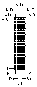
TABLE A-5 shows the J3/P3 connector pin assignments.
TABLE A-5 J3/P3 Connector Pin Assignments
|
Pin #
|
Row Z
|
Row A
|
Row B
|
Row C
|
Row D
|
Row E
|
Row F
|
|
19
|
GND
|
PMC-1
|
PMC-2
|
PMC-3
|
PMC-4
|
PMC-5
|
GND
|
|
18
|
GND
|
PMC-6
|
PMC-7
|
PMC-8
|
PMC-9
|
PMC-10
|
GND
|
|
17
|
GND
|
PMC-11
|
PMC-12
|
PMC-13
|
PMC-14
|
PMC-15
|
GND
|
|
16
|
GND
|
PMC-16
|
PMC-17
|
PMC-18
|
PMC-19
|
PMC-20
|
GND
|
|
15
|
GND
|
PMC-21
|
PMC-22
|
PMC-23
|
PMC-24
|
PMC-25
|
GND
|
|
14
|
GND
|
PMC-26
|
PMC-27
|
PMC-28
|
PMC-29
|
PMC-30
|
GND
|
|
13
|
GND
|
PMC-31
|
PMC-32
|
PMC-33
|
PMC-34
|
PMC-35
|
GND
|
|
12
|
GND
|
PMC-36
|
PMC-37
|
PMC-38
|
PMC-39
|
PMC-40
|
GND
|
|
11
|
GND
|
PMC-41
|
PMC-42
|
PMC-43
|
PMC-44
|
PMC-45
|
GND
|
|
10
|
GND
|
PMC-46
|
PMC-47
|
PMC-48
|
PMC-49
|
PMC-50
|
GND
|
|
9
|
GND
|
PMC-51
|
PMC-52
|
PMC-53
|
PMC-54
|
PMC-55
|
GND
|
|
8
|
GND
|
PMC-56
|
PMC-57
|
PMC-58
|
PMC-59
|
PMC-60
|
GND
|
|
7
|
GND
|
PMC-61
|
PMC-62
|
PMC-63
|
PMC-64
|
VCC
|
GND
|
|
6
|
GND
|
BD_SEL_5#
|
HEALTHY_5#
|
PCI_RST_5#
|
BRSVP
|
BRSVP
|
GND
|
|
5
|
GND
|
BD_SEL_4#
|
HEALTHY_4#
|
PCI_RST_4#
|
BRSVP
|
BRSVP
|
GND
|
|
4
|
GND
|
BD_SEL_3#
|
HEALTHY_3#
|
PCI_RST_3#
|
BRSVP
|
BRSVP
|
GND
|
|
3
|
GND
|
BD_SEL_2#
|
HEALTHY_2#
|
PCI_RST_2#
|
PCIB_RST_L
|
PCI_RST_6#
|
GND
|
|
2
|
GND
|
BD_SEL_1#
|
HEALTHY_1#
|
PCI_RST_1#
|
EP_5V
|
HEALTHY_6#
|
GND
|
TABLE A-6 Signal Definitions
|
PMC[63..0]
|
PMC/PIM I/O signals
|
|
BD_SEL[0..6]#:
|
PICMG Hot-swap Spec 2.1 R1.0 Radial board select bi-directional signals
|
|
HEALTHY[0..6]#:
|
PICMG Hot-swap Spec 2.1 R1.0 Radial board healthy input signals
|
|
PCI_RST[0..6]:
|
PICMG Hot-swap Spec 2.1 R1.0 Radial PCI reset output signals
|
FIGURE A-5 Netra CP2140 Board J4/P4 Connector

TABLE A-7 shows the J4/P4 connector pin assignments.
TABLE A-7 J4/P4 Connector Pin Assignments
|
Pin #
|
Row Z
|
Row A
|
Row B
|
Row C
|
Row D
|
Row E
|
Row F
|
|
25
|
GND
|
MIIA_CRS
|
MIIA_COL
|
MIIA_MDIO_L
|
MIIA_TX_ERS
|
+5V
|
GND
|
|
24
|
GND
|
MIIA_RX_DV
|
MIIA_RX_ER
|
MIIA_TX_CLKI
|
GND
|
BP_MCA_INT_L
|
GND
|
|
23
|
GND
|
MIIA_RXD1
|
MIIA_RXD2
|
GND
|
MIIA_RXD3
|
MII_RX_CLK
|
GND
|
|
22
|
GND
|
GND
|
MIIA_TXD0
|
MIIA_TX_EN
|
MIIA_MDC
|
MIIA_RXD0
|
GND
|
|
21
|
GND
|
MIIA_TXD3
|
GND
|
MIIA_TXD2
|
GND
|
MIIA_TXD1
|
GND
|
|
20
|
GND
|
|
|
LOCAL_I2C_INT_L
|
GND
|
FR/BK_SEL
|
GND
|
|
19
|
GND
|
MIIB_COL
|
MIIB_MDIO_L
|
MIIB_TX_ER
|
|
|
GND
|
|
18
|
GND
|
MIIB_RX_CLK
|
MIIB_RX_DV
|
MIIB_RX_ER
|
MIIB_TX_CLKI
|
MIIB_CRS
|
GND
|
|
17
|
GND
|
MIIB_RXD0
|
GND
|
MIIB_RXD1
|
MIIB_RXD2
|
MIIB_RXD3
|
GND
|
|
16
|
GND
|
MIIB_TXD1
|
MIIB_TXD0
|
MIIB_TX_EN
|
MIIB_MDC
|
GND
|
GND
|
|
15
|
GND
|
GND
|
+5V
|
+5V
|
MIIB_TXD3
|
MIIB_TXD2
|
GND
|
|
14
|
KEY
|
|
|
|
|
|
KEY
|
|
13
|
KEY
|
|
|
|
|
|
KEY
|
|
12
|
KEY
|
|
|
|
|
|
KEY
|
|
11
|
GND
|
BP_TYPE0
|
BP_TYPE1
|
I2C_SDA
|
GND
|
GND
|
GND
|
|
10
|
GND
|
SMC_TX
|
SMC_RX
|
BP_PWROFF
|
(I2C_pwr)
|
+12V
|
GND
|
|
9
|
GND
|
GND
|
GND
|
I2C_SCL
|
TRM_PWR1
|
TRM_PWR2
|
GND
|
|
8
|
GND
|
SCDPH_L
|
SCD<15>_L
|
SCD<14>_L
|
SCD<13>_L
|
SCD<12>_L
|
GND
|
|
7
|
GND
|
SCD<4>_L
|
SCD<3>_L
|
SCD<2>_L
|
SCD<1>_L
|
SCD<0>_L
|
GND
|
|
6
|
GND
|
GND
|
SCDPL_L
|
SCD<7>_L
|
SCD<6>_L
|
SCD<5>_L
|
GND
|
|
5
|
GND
|
GND
|
RSV-MCU-use
|
+5V
|
+5V
|
RSV-MCU-use
|
GND
|
|
4
|
GND
|
SRST_L
|
ACK_L
|
BSY_L
|
GND
|
ATN_L
|
GND
|
|
3
|
GND
|
I/O_L
|
REQ_L
|
C/D_L
|
SEL_L
|
MSG_L
|
GND
|
|
2
|
GND
|
Term_Disable
|
SCD<11>_L
|
SCD<10>_L
|
SCD<9>_L
|
SCD<8>_L
|
GND
|
|
1
|
GND
|
RSV-MCU-use
|
RSV-MCU-use
|
+3.3V
|
-12V
|
GPIO1-RSV-MCU-use
|
GND
|
TABLE A-8 Signal Definitions
|
BP_MCA_INT_L:
|
Reserved for MC system use
|
|
LOCAL_I2C_INT_L:
|
I2C interrupt signals for CP2140 I2C devices
|
|
BP_TYPE[0..1]:
|
Intended to indicate backplane type (HA, FHS, Non-HA, etc) - not supported
|
|
SMC_TX/RX:
|
SMC tty signals
|
|
BP_PWROFF:
|
When OS level init 5 is executed - system is halted and this signal asserted logic level high
|
|
I2C_PWR:
|
I2C power for CP2140 local I2C devices
|
|
I2C_SCL/SDA:
|
CP2140 local I2C clock/data
|
TABLE A-9 MII Signals
|
MII_RXD<0:3>:
|
Receive data
|
|
MII_TXD<0:3>:
|
Transmit data
|
|
MII_RX_CLK:
|
Receive clock
|
|
MII_TX_CLKI:
|
Transmit clock
|
|
MII_TX_EN:
|
Transmit enable
|
|
MII_CRS:
|
Carrier sense
|
|
MII_COL:
|
Collision detect
|
|
MII_RX_ER:
|
Receive error
|
|
MII_TX_ER:
|
Transmit error
|
|
MII_RX_DV:
|
Receive frame detect
|
|
MII_MDIO:
|
Transceiver management data (external)
|
TABLE A-10 SCSI single-ended levels - SCSI-A on J4 and SCSI-B on J5
|
ATN:
|
Attention - Active low n BSY: Busy - Active low
|
|
C/D:
|
Command or Data - Active low
|
|
I/O:
|
Input or output data direction
|
|
MSG:
|
Message phase indicator - active low
|
|
ACK:
|
Acknowledge - Active low
|
|
SCD<0:15>:
|
SCSI data lines - Active low
|
|
SCDPHSCSI :
|
parity high byte; provides parity for SCD[8:15] - Active low
|
|
SCDPLSCSI:
|
parity low byte; provides parity for SCD[0:7] - Active low
|
|
SEL:
|
Select - Active low
|
|
REQ:
|
Request - Active low
|
|
SRST:
|
SCSI bus reset - Active low
|
|
TRM_PWR:
|
Termination power for external SCSI terminator
|
FIGURE A-6 shows the Netra CP2140 Board J5/P5 Connector.
FIGURE A-6 Netra CP2140 Board J5/P5 Connector
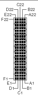
TABLE A-11 shows the Netra CP2140 board J5/P5 Connector Pin Assignments.
TABLE A-11 J5/P5 Connector Pin Assignments
|
Pin #
|
Row Z
|
Row A
|
Row B
|
Row C
|
Row D
|
Row E
|
Row F
|
|
22
|
GND
|
BKRST_IN_L
|
GND
|
DIAG_L_OC
|
+5V
|
BP_XIR_L
|
GND
|
|
21
|
GND
|
KBDDAT
|
KBDCLK
|
KBDVCC
|
AUXDATA
|
AUXCLK
|
GND
|
|
20
|
GND
|
+5V
|
UBS1_P
|
USB1_N
|
KBDGND
|
INT_2#
|
GND
|
|
19
|
GND
|
STB_L
|
GND
|
VCC
|
INT_0#
|
INT_1#
|
GND
|
|
18
|
GND
|
AFD_L
|
USB2_P
|
USB2_N
|
GND
|
+5V
|
GND
|
|
17
|
GND
|
PD<2>
|
INIT_L
|
PD<1>
|
ERR
|
PD<0>
|
GND
|
|
16
|
GND
|
PD<6>
|
PD<5>
|
PD<4>
|
PD<3>
|
SLIN_L
|
GND
|
|
15
|
GND
|
SLCT
|
PE
|
BUSY_L
|
ACK_L
|
PD<7>
|
GND
|
|
14
|
GND
|
RTSA
|
CTSA
|
RIA
|
GND
|
DTRA
|
GND
|
|
13
|
GND
|
DCDA
|
+5V
|
RXDA
|
DSRA
|
TXDA
|
GND
|
|
12
|
GND
|
RTSB
|
CTSB
|
RIB
|
+5V
|
DTRB
|
GND
|
|
11
|
GND
|
DCDB
|
GND
|
RXDB
|
DSRB
|
TXDB
|
GND
|
|
10
|
GND
|
TR0_L
|
WPROT_L
|
RDATA_L
|
HDSEL_L
|
DSKCHG_L
|
GND
|
|
9
|
GND
|
MTR1_L
|
DIR_L
|
STEP_L
|
WDATA_L
|
WGATE_L
|
GND
|
|
8
|
GND
|
DRVDENS1
|
INDEX_L
|
MTR0_L
|
DS1_L
|
DS0_L
|
GND
|
|
7
|
GND
|
DRATE0
|
SC2D<2>_L
|
SC2D<1>_L
|
SC2D<0>_L
|
DRVDENS0
|
GND
|
|
6
|
GND
|
SC2D<6>_L
|
GND
|
SC2D<5>_L
|
SC2D<4>_L
|
SC2D<3>_L
|
GND
|
|
5
|
GND
|
SC2D<10>_L
|
SC2D<9>_L
|
SC2D<8>_L
|
SC2DPL_L
|
SC2D<7>_L
|
GND
|
|
4
|
GND
|
SC2D<13>_L
|
SC2D<12>_L
|
GND
|
MSEN0
|
SC2D<11>_L
|
GND
|
|
3
|
GND
|
Term_Disable
|
SC2DPH_L
|
SC2D<15>_L
|
MSEN1
|
SC2D<14>_L
|
GND
|
|
2
|
GND
|
I/O2_L
|
REQ2_L
|
C/D2_L
|
SEL2_L
|
MSG2_L
|
GND
|
|
1
|
GND
|
BKRST_OUT_L
|
SRST2_L
|
ACK2_L
|
BUSY2_L
|
ATN2_L
|
GND
|
TABLE A-12 Miscellaneous
|
BKRST_IN_L:
|
Backplane reset input to SMC
|
|
BKRST_OUT_L:
|
Backplane test output from SMC
|
|
BP_XIR_L:
|
Push button reset system input. Active low
|
|
DIAG_LOC:
|
Diagnostic / Alarm output from SMC
|
TABLE A-13 USB Signals
|
USB1_P/N:
|
USB (Universal Serial Bus) signal pair - RIO-A
|
|
USB2_P/N:
|
USB (Universal Serial Bus) signal pair - RIO-B
|
|
INT[0..2]:
|
cPCI interface signal interrupts, not supported
|
TABLE A-14 Parallel Port
|
ACK_L:
|
Pulsed by peripheral to acknowledge data sent
|
|
BUSY:
|
Indicates a printer cannot accept more data
|
|
ERR_L:
|
Peripheral detected an error
|
|
PD[7..0]:
|
Parallel data lines
|
|
PE:
|
Paper end - indicates printer is out of paper
|
|
AFD_L:
|
auto feed - causes printer to line feed
|
|
INIT_L:
|
initializes the peripheral
|
|
SLIN_L:
|
select in - selects the peripheral
|
|
STB_L:
|
data strobe - indicates data is valid
|
|
SLCT:
|
select, peripheral indicates it is selected
|
TABLE A-15 Serial COM Ports (A and B), RS 232 Levels
|
CTS:
|
clear to send
|
|
DCD:
|
Data Carrier Detected
|
|
DSR:
|
Data Set Ready
|
|
DTR:
|
Data Terminal Ready
|
|
RI:
|
Ring Indicator
|
|
RTS:
|
Request to Send
|
|
RXD:
|
Serial Receive Data
|
|
TXD:
|
Serial Transmit Data
|
TABLE A-16 Floppy Disk Drive, TTL Levels
|
DSKCHG_L:
|
indicates the drive door has been opened
|
|
DIR_L:
|
controls direction of the head during step operations
|
|
DRATE[0]:
|
reflects the value of the data transfer but in the DSR or CCR
|
|
DRVDENS[1..0]:
|
disk density select communication in rev1.0, resvd in 1.1 n DS[1..0]: drive selects
|
|
HDSEL_L:
|
selects top or bottom side head
|
|
INDEX_L:
|
indicates the beginning of a track
|
|
MSEN[1..0]:
|
used for sensing density of the media
|
|
RDATA_L:
|
data read
|
|
STEP_L:
|
step, pulses move head in or out
|
|
TR0_L:
|
indicates the is positioned above track 00
|
|
WDATA_L:
|
write data to drive
|
|
WGATE_L:
|
enables head write circuitry of drive
|
|
WPROT_L:
|
indicates a disk is write-protected
|
TABLE A-17 Keyboard/Auxiliary Device Signals
|
AUXCLK:
|
Clock for PS/2 auxiliary device (mouse) - TTL levels, active high
|
|
AUXDAT:
|
Serial data line for PS/2 auxiliary device (mouse) - TTL levels, active high
|
|
KBDCLK:
|
Clock for PC/AT or PS/2 keyboard - TTL levels, active high
|
|
KBDDAT:
|
Serial data line for PC/AT or PS/2 keyboard - TTL levels, active high
|
A.1.1 Mini Din 8-Pin Connector
FIGURE A-7 Serial Connector- Mini Din 8-Pin Front Panel TTYA Diagram
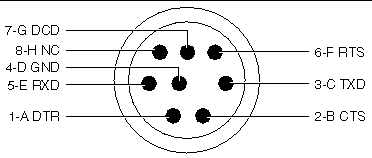
TABLE A-18 shows the Mini Din 8-pin connector pinouts.
TABLE A-18 Serial Mini Din 8-pin Connector Pinouts
|
Pin
|
Signal Name
|
|
Pin
|
Signal Name
|
|
1
|
FP_SER_A_DTR
|
|
5
|
FP_SER_A_RXD
|
|
2
|
FP_SER_A_CTS
|
|
6
|
FP_SER_A_RTS
|
|
3
|
FP_SER_A_TXD
|
|
7
|
FP_SER_A_DCD
|
|
4
|
FP_SER_A_GND
|
|
8
|
GND
|
A.1.2 RJ45 Connector
The twisted pair Ethernet connector is a RJ45 connector. The controller auto-negotiates to either 10Base-T or 100Base-T. The pinout shown in TABLE A-19 applies to all of the Ethernet.
FIGURE A-8 RJ45 Ethernet Connector Diagram
TABLE A-19 shows the Netra CP2140 board front panel Ethernet connector.
TABLE A-19 Netra CP2140 Board Front Panel Ethernet Connector Pinout
|
Pin #
|
Description
|
|
1
|
TXD+
|
|
2
|
TXD-
|
|
3
|
RXD+
|
|
4
|
4T_D3P
|
|
5
|
4T_D3P
|
|
6
|
RXD-
|
|
7
|
4T_D4P
|
|
8
|
4T_D4P
|
A.1.3 PMC Connectors
FIGURE A-9 shows the PMC connectors: J3001, J3002, and J3003.
FIGURE A-9 J3001-J3003 Connectors
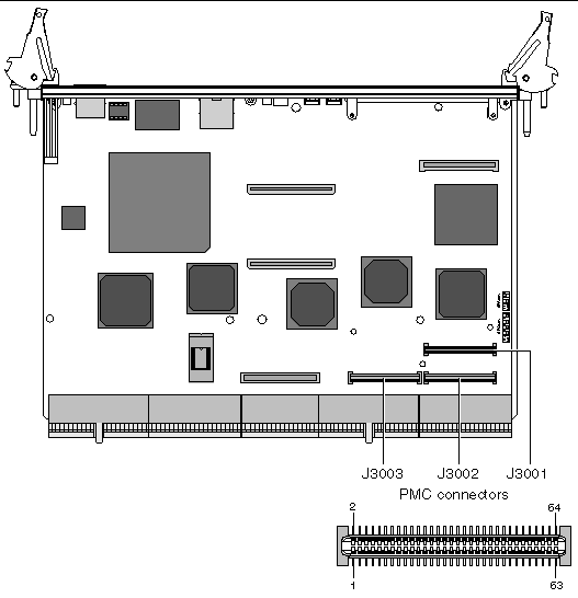
TABLE A-20 shows the connector pinouts for the J3001 connector.
TABLE A-20 PMC J3001 Connector Pinouts
|
Pin
|
Voltage
|
|
Pin
|
Voltage
|
|
1
|
TCK
|
|
2
|
-12V
|
|
3
|
GND
|
|
4
|
INTA
|
|
5
|
INTB
|
|
6
|
INTC
|
|
7
|
BUSMODE1
|
|
8
|
+5V
|
|
9
|
INTD
|
|
10
|
PCI_RSVD
|
|
11
|
GND
|
|
12
|
PCI_RSVD
|
|
13
|
CLK
|
|
14
|
GND
|
|
15
|
GND
|
|
16
|
GNT
|
|
17
|
REQ
|
|
18
|
+5V
|
|
19
|
V(I/O)
|
|
20
|
AD31
|
|
21
|
AD28
|
|
22
|
AD27
|
|
23
|
AD25
|
|
24
|
GND
|
|
25
|
GND
|
|
26
|
CBE3
|
|
27
|
AD22
|
|
28
|
AD21
|
|
29
|
AD19
|
|
30
|
+5V
|
|
31
|
V (IO)
|
|
32
|
AD17
|
|
33
|
FRAME
|
|
34
|
GND
|
|
35
|
GND
|
|
36
|
IRDY
|
|
37
|
DEVSEL
|
|
38
|
+5V
|
|
39
|
GND
|
|
40
|
LOCK
|
|
41
|
SDONE
|
|
42
|
SBO
|
|
43
|
PAR
|
|
44
|
GND
|
|
45
|
V (IO)
|
|
46
|
AD15
|
|
47
|
AD12
|
|
48
|
AD11
|
|
49
|
AD9
|
|
50
|
+5V
|
|
51
|
GND
|
|
52
|
CBE0
|
|
53
|
AD6
|
|
54
|
AD5
|
|
55
|
AD4
|
|
56
|
GND
|
|
57
|
V (IO)
|
|
58
|
AD3
|
|
59
|
AD2
|
|
60
|
AD1
|
|
61
|
AD0
|
|
62
|
+5V
|
|
63
|
GND
|
|
64
|
REQ64
|
A.1.4 PMC J3002 Connector
TABLE A-21 PMC J3002 Connector Pinouts
|
Pin
|
Voltage
|
|
Pin
|
Voltage
|
|
1
|
+12V
|
|
2
|
TRST
|
|
3
|
TMS
|
|
4
|
TD0
|
|
5
|
TD1
|
|
6
|
GND
|
|
7
|
GND
|
|
8
|
PCI_RSVD
|
|
9
|
PCI_RSVD
|
|
10
|
PCI_RSVD
|
|
11
|
BUSMODE2
|
|
12
|
+3.3V
|
|
13
|
RST
|
|
14
|
BUSMODE3
|
|
15
|
+3.3V
|
|
16
|
BUSMODE4
|
|
17
|
PCI_RSVD
|
|
18
|
GND
|
|
19
|
AD30
|
|
20
|
AD29
|
|
21
|
GND
|
|
22
|
AD26
|
|
23
|
AD24
|
|
24
|
3.3V
|
|
25
|
IDSEL
|
|
26
|
AD23
|
|
27
|
+3.3V
|
|
28
|
AD20
|
|
29
|
AD18
|
|
30
|
GND
|
|
31
|
AD16
|
|
32
|
CBE2
|
|
33
|
GND
|
|
34
|
PMC_RSVD
|
|
35
|
TRDY
|
|
36
|
+3.3V
|
|
37
|
GND
|
|
38
|
STOP
|
|
39
|
PERR
|
|
40
|
GND
|
|
41
|
+3.3V
|
|
42
|
SERR
|
|
43
|
CBE1
|
|
44
|
GND
|
|
45
|
AD14
|
|
46
|
AD13
|
|
47
|
GND
|
|
48
|
AD10
|
|
49
|
AD8
|
|
50
|
+3.3V
|
|
51
|
AD7
|
|
52
|
PMC_RSVD
|
|
53
|
+3.3V
|
|
54
|
PMC_RSVD
|
|
55
|
PMC_RSVD
|
|
56
|
GND
|
|
57
|
PMC_RSVD
|
|
58
|
PMC_RSVD
|
|
59
|
GND
|
|
60
|
PMC_RSVD
|
|
61
|
ACK64
|
|
62
|
+3.3V
|
|
63
|
GND
|
|
64
|
PMC_RSVD
|
A.1.5 PMC J3003 Connector
TABLE A-22 PMC J3003 Connector Pinouts
|
Pin
|
Voltage
|
|
Pin
|
Voltage
|
|
1
|
IO1
|
|
2
|
IO2
|
|
3
|
IO3
|
|
4
|
IO4
|
|
5
|
IO5
|
|
6
|
IO6
|
|
7
|
IO7
|
|
8
|
IO8
|
|
9
|
IO9
|
|
10
|
IO10
|
|
11
|
IO11
|
|
12
|
IO12
|
|
13
|
IO13
|
|
14
|
IO14
|
|
15
|
IO15
|
|
16
|
IO16
|
|
17
|
IO17
|
|
18
|
IO18
|
|
19
|
IO19
|
|
20
|
IO20
|
|
21
|
IO21
|
|
22
|
IO22
|
|
23
|
IO23
|
|
24
|
IO24
|
|
25
|
IO25
|
|
26
|
IO26
|
|
27
|
IO27
|
|
28
|
IO28
|
|
29
|
IO29
|
|
30
|
IO30
|
|
31
|
IO31
|
|
32
|
IO32
|
|
33
|
IO33
|
|
34
|
IO34
|
|
35
|
IO35
|
|
36
|
IO36
|
|
37
|
IO37
|
|
38
|
IO38
|
|
39
|
IO39
|
|
40
|
IO40
|
|
41
|
IO41
|
|
42
|
IO42
|
|
43
|
IO43
|
|
44
|
IO44
|
|
45
|
IO45
|
|
46
|
IO46
|
|
47
|
IO47
|
|
48
|
IO48
|
|
49
|
IO49
|
|
50
|
IO50
|
|
51
|
IO51
|
|
52
|
IO52
|
|
53
|
IO53
|
|
54
|
IO54
|
|
55
|
IO55
|
|
56
|
IO56
|
|
57
|
IO57
|
|
58
|
IO58
|
|
59
|
IO59
|
|
60
|
IO60
|
|
61
|
IO61
|
|
62
|
IO62
|
|
63
|
IO63
|
|
64
|
IO64
|
FIGURE A-10 shows the location of memory module connectors J0601 and J0602, respectively.
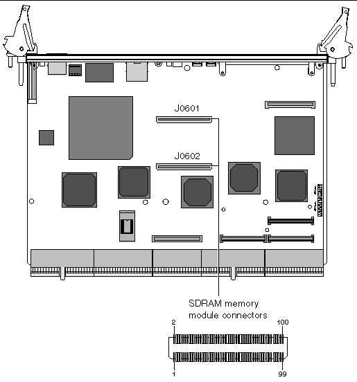
FIGURE A-10 Memory Module Connectors J0601 and J0602
A.2 Memory Module Connector Pinout
TABLE A-23 and TABLE A-24 show the memory module connector 1 and 2 pinouts.
TABLE A-23 Memory Module Connector 1 Pinout (Bottom Side)
|
Pin #
|
Front Side
|
Pin #
|
Front Side
|
Pin #
|
Back Side
|
Pin #
|
Back Side
|
|
99
|
VDD_3.3V
|
49
|
AB3
|
100
|
VSS
|
50
|
DQ9
|
|
97
|
DQ43
|
47
|
AA2
|
98
|
DQ0
|
48
|
DQ10
|
|
95
|
DQ42
|
45
|
VSS
|
96
|
DQ1
|
46
|
VDD_3.3V
|
|
93
|
DQ41
|
43
|
AB2
|
94
|
DQ2
|
44
|
DQ11
|
|
91
|
VSS
|
41
|
AA1
|
92
|
VDD_3.3V
|
42
|
DQ12
|
|
89
|
DQ40
|
39
|
AB1
|
90
|
DQ3
|
40
|
DQ13
|
|
87
|
DQ35
|
37
|
VDD_3.3V
|
88
|
DQ4
|
38
|
VSS
|
|
85
|
VDD_3.3V
|
35
|
AA0
|
86
|
VSS
|
36
|
DQ14
|
|
83
|
DQ34
|
33
|
AB0
|
84
|
DQ5
|
34
|
DQ15
|
|
81
|
DQ33
|
31
|
VSS
|
82
|
DQ6
|
32
|
VDD_3.3V
|
|
79
|
DQ32
|
29
|
CK3
|
80
|
DQ7
|
30
|
CK1
|
|
77
|
VSS
|
27
|
VDD_3.3V
|
78
|
VDD_3.3V
|
28
|
VSS
|
|
75
|
CK2
|
25
|
S1
|
76
|
CK0
|
26
|
S0
|
|
73
|
VSS
|
23
|
S5
|
74
|
RAS0
|
24
|
S4
|
|
71
|
NC
|
21
|
DQ27
|
72
|
RAS2
|
22
|
DQ16
|
|
69
|
VDD_3.3V
|
19
|
DQ26
|
70
|
VSS
|
20
|
DQ17
|
|
67
|
AA6
|
17
|
VSS
|
68
|
CAS0
|
18
|
VDD_3.3V
|
|
65
|
AB6
|
15
|
DQ25
|
66
|
CAS2
|
16
|
DQ18
|
|
63
|
AA5
|
13
|
DQ24
|
64
|
WE0
|
14
|
DQ19
|
|
61
|
VSS
|
11
|
ALERT
|
62
|
VDD_3.3V
|
12
|
DQ20
|
|
59
|
AB5
|
9
|
VDD_3.3V
|
60
|
WE2
|
10
|
VSS
|
|
57
|
AA4
|
7
|
SA2
|
58
|
CKE0
|
8
|
DQ21
|
|
55
|
AB4
|
5
|
SA1
|
56
|
CKE2
|
6
|
DQ22
|
|
53
|
VDD_3.3V
|
3
|
NC
|
54
|
VSS
|
4
|
DQ23
|
|
51
|
AA3
|
1
|
VDD_3.3VI2C
|
52
|
DQ8
|
2
|
VDD_3.3V
|
TABLE A-24 Memory Module Connector 2 Pinout (Bottom Side)
|
Pin #
|
Front Side
|
Pin #
|
Front Side
|
Pin #
|
Back Side
|
Pin #
|
Back Side
|
|
99
|
VSS
|
49
|
DQ62
|
100
|
VDD_3.3V
|
50
|
AB10
|
|
97
|
DQ71
|
47
|
DQ61
|
98
|
DQ47
|
48
|
AA9
|
|
95
|
DQ70
|
45
|
VDD_3.3V
|
96
|
DQ46
|
46
|
VSS
|
|
93
|
DQ69
|
43
|
DQ60
|
94
|
DQ45
|
44
|
AB9
|
|
91
|
VDD_3.3V
|
41
|
DQ59
|
92
|
VSS
|
42
|
AA8
|
|
89
|
DQ68
|
39
|
DQ58
|
90
|
DQ44
|
40
|
AB8
|
|
87
|
DQ67
|
37
|
VSS
|
88
|
DQ39
|
38
|
VDD_3.3V
|
|
85
|
VSS
|
35
|
DQ57
|
86
|
VDD_3.3V
|
36
|
AA7
|
|
83
|
DQ66
|
33
|
DQ56
|
84
|
DQ38
|
34
|
AB7
|
|
81
|
DQ65
|
31
|
VDD_3.3V
|
82
|
DQ37
|
32
|
VSS
|
|
79
|
DQ64
|
29
|
CK4
|
80
|
DQ36
|
30
|
CK6
|
|
77
|
VDD_3.3V
|
27
|
VSS
|
78
|
VSS
|
28
|
VDD_3.3V
|
|
75
|
CK5
|
25
|
S3
|
76
|
CK7
|
26
|
S2
|
|
73
|
RAS1
|
23
|
S7
|
74
|
BAA1
|
24
|
S6
|
|
71
|
RAS3
|
21
|
DQ55
|
72
|
BAB1
|
22
|
DQ31
|
|
69
|
VSS
|
19
|
DQ54
|
70
|
VDD_3.3V
|
20
|
DQ30
|
|
67
|
CAS1
|
17
|
VDD_3.3V
|
68
|
BAA0
|
18
|
VSS
|
|
65
|
CAS3
|
15
|
DQ53
|
66
|
BAB0
|
16
|
DQ29
|
|
63
|
WE1
|
13
|
DQ52
|
64
|
AA12
|
14
|
DQ28
|
|
61
|
VDD_3.3V
|
11
|
DQ51
|
62
|
VSS
|
12
|
LCLK-I
|
|
59
|
WE3
|
9
|
VDD_3.3V
|
60
|
AB12
|
10
|
VSS
|
|
57
|
CKE1
|
7
|
DQ50
|
58
|
AA11
|
8
|
LCLK-O
|
|
55
|
CKE3
|
5
|
DQ49
|
56
|
AB11
|
6
|
SDA
|
|
53
|
VSS
|
3
|
DQ48
|
54
|
VDD_3.3V
|
4
|
SCK
|
|
51
|
DQ63
|
1
|
VDD_3.3V
|
52
|
AA10
|
2
|
VSS
|
A.3 SMC Switch Settings for HA and Non-HA Systems
The switches on the CP2140 SMC Module serve two purposes:
- Establish backplane type (HA or non-HA)
- Select Boot Device (Boot Flash or SMC config block setting)
SW0501.Switch1 is for HA/Non-HA settings and SW0501.Switch2 is for flash device selection based on SMC settings.
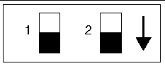
A.3.1 Setting Non-HA Systems
If you have a non-HA system, set the SMC module switch settings before powering on the Netra CP2140 board unit.
- SW0501.Switch1 ---> Closed (switch is set in the direction of the arrow)
- SW0501.Switch2 ---> Closed (switch is set in direction of arrow)
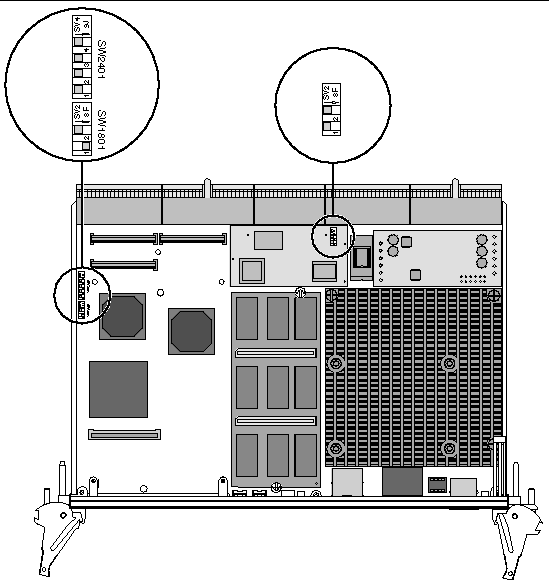
See FIGURE A-11 for the location of SW0501 on the Netra CP2140 board.
FIGURE A-11 Setting Switches to Closed Position
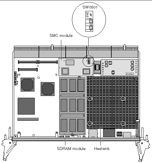
FIGURE A-12 SW0501 Position for non-HA Systems
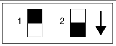
A.3.2 Setting HA Systems
If the user has a HA system, set the SMC switch settings before powering on the CP2140 unit as follows:
- SW0501.Switch1 ---> Open (switch is set opposite to arrow direction)
- SW0501.Switch2 ---> Closed (switch is set in direction of arrow)
See FIGURE A-13 for location of SW0501.
FIGURE A-13 Location of SW0501 on SMC Module

FIGURE A-14 shows how to set switch positions for HA systems.
FIGURE A-14 SW0501 Switch Setting for HA Systems
A.4 SCSI and Flash Switch Settings
Two sets of switches on the Netra CP2140 board perform two different functions:
- SW1801 for flash device selection
- SW2401 for SCSI termination
The positions of these switches determine the flash device selection and SCSI termination. If a switch is moved in the direction of the arrow, it is closed (ON). If a switch is moved in the opposite direction of the arrow, it is open (OFF). FIGURE A-15 shows switches and the switch setting legend.
|
Note - The default for both the SW2401 and SW1801 switches is Open/Off.
|
FIGURE A-15 Switch Setting Legend
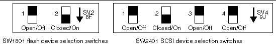
A.4.1 Flash Device Selection Switches
The position of the two SW1801 switches determines the flash device selection on the board. TABLE A-26 describes the flash device selection.
TABLE A-25 Flash Device Switch Setting (SW1801)
|
Position Switch No. 1
|
Position Switch No. 2
|
Description
|
|
Open
|
Open
|

OBP 1 MB boot flash selected (default)
Should never be user adjusted
|
|
Closed
|
Closed
|

User flash 1 selected
|
|
Open
|
Closed
|

User flash 1 and 2 selected
|
A.4.2 SCSI Termination Switches
Four SW2401 SCSI termination switches are located on the board.
The SCSI switches operate independently from each other and can be set to Open or Closed position. FIGURE A-16 shows an example of SCSI termination switch settings.
FIGURE A-16 SCSI Termination Switch Setting Example
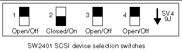
TABLE A-26 describes the SCSI termination switch setting.
TABLE A-26 SCSI Termination Switch Setting (SW2401)
|
Position
|
Switch 1
|
Switch 2
|
Switch 3
|
Switch 4
|
|
Open
|
Termination power supplied for SCSI Bus A.
|
Termination power supplied for SCSI Bus B.
|
Termination enabled for SCSI Bus A.
|
Termination enabled for SCSI Bus B.
|
|
Closed
|
Termination power not supplied for SCSI Bus A.
|
Termination power not supplied for SCSI Bus B.
|
Termination disabled for SCSI Bus A.
|
Termination disabled for SCSI Bus B.
|
See FIGURE A-17 for the location of flash device, SCSI, and SMC FPGA (SW0501) switches.
FIGURE A-17 SCSI Switch Selections and SMC on the Netra CP2140 Board