| Sun Blade X6220 Server Module Service Manual
|
    |
This appendix contains information about the following connector pinouts:
C.1 Front I/O Dongle
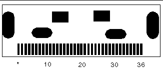
The front I/O dongle connector pins and their corresponding descriptions are shown in the figure and table in this section.
FIGURE C-1 Front I/O Dongle Connector

TABLE C-1 Front I/O Dongle Pins
|
Signal Name
|
Pin #
|
Pin #
|
Signal Name
|
|
No Connect
|
1, 21, 28, 30, 31, 33, 34
|
15
|
USB0_FRONT_VCC
|
|
DNGL_VGA_RED
|
2
|
16
|
USB1_FRONT_VCC
|
|
DNGL_VGA_GRN
|
3
|
17
|
USB1_FRONT_VCC
|
|
DNGL_VGA_BLU
|
4
|
18
|
USB1_FRONT_CM_N
|
|
GND
|
5
|
19
|
USB1_FRONT_CM_P
|
|
DNGL_VGA_MONID2
|
6
|
20
|
GND
|
|
GND
|
7, 11, 20, 29, 32, 36
|
22
|
DNGL_RES_SER_RXD
|
|
DNGL_VGA_MONID1
|
8
|
23
|
RES_DNGL_SER_RTS_N
|
|
DNGL_VGA_HSYNC_BUF
|
9
|
24
|
RES_DNGL_SER_TXD
|
|
DNGL_VGA_VSYNC_BUF
|
10
|
25
|
DNGL_RES_SER_CTS_N
|
|
GND
|
11
|
26
|
RES_DNGL_SER_DTR_N
|
|
USB0_FRONT_CM_N
|
12
|
27
|
DNGL_RES_SER_DCD_N
|
|
USB0_FRONT_CM_P
|
13
|
35
|
DONGLE_PRSNT_L
|
|
USB0_FRONT_VCC
|
14
|
|
|
C.2 SAS Connectors
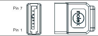
The Serial Attached SCSI (SAS) connector pins and their corresponding descriptions are shown in the figure and table in this section.
FIGURE C-2 SAS Connector

TABLE C-2 SAS Connector Pins
|
Segment
|
Pin Number
|
Pin Name
|
Description
|
|
Signal Segment
|
S1
|
Gnd
|
Second mate ground
|
|
S2
|
TX+
|
Positive side of transmit to hard drive
|
|
S3
|
TX-
|
Negative side of transmit to hard drive
|
|
S4
|
Gnd
|
Second mate ground
|
|
S5
|
RX-
|
Negative side of receive from hard drive
|
|
S6
|
RX+
|
Positive side of receive from hard drive
|
|
S7
|
Gnd
|
Second mate ground
|
|
Backside Signal Segment
|
S8
|
Gnd
|
Second mate ground
|
|
S9
|
|
Not used
|
|
S10
|
|
Not used
|
|
S11
|
Gnd
|
Second mate ground
|
|
S12
|
|
Not used
|
|
S13
|
|
Not used
|
|
S14
|
Gnd
|
Second mate ground
|
|
Power Segment
|
P1
|
3.3 V
|
Not used
|
|
P2
|
3.3 V
|
Not used
|
|
P3
|
3.3 V
|
Not used
|
|
P4
|
Gnd
|
First mate ground
|
|
P5
|
Gnd
|
Second mate ground
|
|
P6
|
Gnd
|
Second mate ground
|
|
P7
|
5.0 V
|
Pre-charge, second mate
|
|
P8
|
5.0 V
|
|
|
P9
|
5.0 V
|
|
|
P10
|
Gnd
|
Second mate ground
|
|
P11
|
Reserved
|
Should be grounded
|
|
P12
|
Gnd
|
First mate ground
|
|
P13
|
12.0 V
|
Pre-charge, second mate
|
|
P14
|
12.0 V
|
|
|
P15
|
12.0 V
|
|
C.3 Service Processor Module
The service processor module connector pins and their corresponding descriptions are shown in the figure and table in this section.
FIGURE C-3 Service Processor Module Connector

TABLE C-3 Service Processor Module Connector Pins
|
Signal Name
|
Pin #
|
Pin #
|
Signal Name
|
|
V33Aux
|
1
|
2
|
GND
|
|
GPIOS1
|
3
|
4
|
SP_I2C_CLK
|
|
GPIOS0
|
5
|
6
|
SP_I2C_DAT
|
|
HOST_LPC_RESET_L
|
7
|
8
|
V3_3AUX
|
|
PPC_WANTS_LPC_L
|
9
|
10
|
SP_TDI
|
|
GND
|
11
|
12
|
SP_TDO
|
|
PS3_POWEROK
|
13
|
14
|
SP_TCK
|
|
PS2_POWEROK
|
15
|
16
|
SP_TMS
|
|
PS1_POWEROK
|
17
|
18
|
SP_TRST_L
|
|
PS0_POWEROK
|
19
|
20
|
GND
|
|
GND
|
21
|
22
|
ALL_POWERGOOD
|
|
PCI_MFG_SCAN_L (for Sparc)
|
23
|
24
|
TOGGLE_POWER
|
|
AFT_MODE_L (for Sparc)
|
25
|
26
|
SP_SCAN_ENABLE_L
|
|
V5V
|
27
|
28
|
SP_OK
|
|
LPC_LAD3
|
29
|
30
|
SYS_HEARTBEAT
|
|
LPC_LAD2
|
31
|
32
|
GND
|
|
LPC_LAD1
|
33
|
34
|
LPC_SER_IRQ
|
|
LPC_LAD0
|
35
|
36
|
SERIAL_CNTL
|
|
LPC_FRAME_L
|
37
|
38
|
PROC_I2C_DISABLE
|
|
GND
|
39
|
40
|
NMI_DUMP_L
|
|
LPC_CLK
|
41
|
42
|
LOCATE_L
|
|
GND
|
43
|
44
|
SYS_SP_RESET_L
|
|
V33AUX
|
45
|
46
|
V3_3
|
|
USB2_P
|
47
|
48
|
SP_FORCE_OFF
|
|
USB2_N
|
49
|
50
|
SP_PWR_ON_RESET_L
|
|
GND
|
51
|
52
|
SP_INSTALLED_L
|
|
USB1_P
|
53
|
54
|
SP_LDSTOP_L
|
|
USB1_N
|
55
|
56
|
BASE_SP_BUTTON
|
|
GND
|
57
|
58
|
GND
|
|
USB0_P
|
59
|
60
|
PPC_TX3
|
|
USB0_N
|
61
|
62
|
PPC_RX3
|
|
GND
|
63
|
64
|
V33AUX
|
|
DVI_RX0_P
|
65
|
66
|
SOL_RXD
|
|
DVI_RX0_N
|
67
|
68
|
SOL_TXD
|
|
GND
|
69
|
70
|
SOL_CTS_L
|
|
DVI_RX1_P
|
71
|
72
|
SOL_DCD_L
|
|
DVI_RX1_N
|
73
|
74
|
SOL_DTR_L
|
|
GND
|
75
|
76
|
SOL_RTS_L
|
|
DVI_RX2_P
|
77
|
78
|
GND
|
|
DVI_RX2_N
|
79
|
80
|
PPC_RXD
|
|
GND
|
81
|
82
|
PPC_TXD
|
|
DVI_RXC_P
|
83
|
84
|
PPC_CTS_L
|
|
DVI_RXC_N
|
85
|
86
|
PPC_DCD_L
|
|
GND
|
87
|
88
|
PPC_DTR_L
|
|
ETH_RX_P
|
89
|
90
|
PPC_RTS_L
|
|
ETH_RX_N
|
91
|
92
|
GND
|
|
GND
|
93
|
94
|
Eth_Rx_Act
|
|
ETH_TX_P
|
95
|
96
|
Eth_Link_1000
|
|
ETH_TX_N
|
97
|
98
|
Eth_Link_100
|
|
GND
|
99
|
100
|
V33AUX
|
C.4 SAS Diskplane
The SAS diskplane connector pins and their corresponding descriptions are shown in the figures and tables in this section.
FIGURE C-4 SAS Diskplane Signal Connector

TABLE C-4 SAS Disk Backplane Signal Connector Pins
|
Pin Number
|
Signal Name
|
|
1, 4, 7
|
GND
|
|
2, 3
|
TX+/TX-
|
|
5, 6
|
RX+/RX-
|
C.5 SAS Power/LED Connector
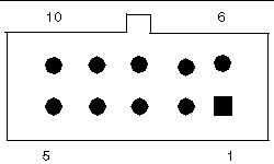
The SAS power/LED connector pins and their corresponding descriptions are shown in the figures and tables in this section.
FIGURE C-5 SAS Power/LED Connector

TABLE C-5 SAS Power/LED Connector Pins
|
Pin Number
|
Signal Name
|
|
1
|
DISK1_FAULT_LED_N
|
|
2
|
DISK1_RDY2RM_N
|
|
3
4
5
6
|
DISK1_ACT_LED_N
12V
GND
DISK0_FAULT_LED_N
|
|
7
|
DISK0_RDY2RM_N
|
|
8
|
DISK0_ACT_LED_N
|
|
9
|
5V
|
|
10
|
GND
|
C.6 Compact Flash
The Compact Flash connector pins and their corresponding descriptions are shown in the figures and tables in this section.
FIGURE C-6 Compact Flash Connector

TABLE C-6 Compact Flash Connector Pins
|
Signal Name
|
Pin #
|
Pin #
|
Signal Name
|
|
GND
|
1
|
26
|
PRSNT_N
|
|
D03
|
2
|
27
|
D11
|
|
D04
|
3
|
28
|
D12
|
|
D05
|
4
|
29
|
D13
|
|
D06
|
5
|
30
|
D14
|
|
D07
|
6
|
31
|
D15
|
|
CS1_L
|
7
|
32
|
CS3_L
|
|
GND
|
8
|
33
|
No Connect
|
|
ATA_SEL
|
9
|
34
|
IOR_L
|
|
GND
|
10
|
35
|
IOW_L
|
|
GND
|
11
|
36
|
WE
|
|
GND
|
12
|
37
|
INT_L
|
|
3.3V
|
13
|
38
|
3.3V
|
|
GND
|
14
|
39
|
IDE_CSEL
|
|
GND
|
15
|
40
|
No Connect
|
|
GND
|
16
|
41
|
IDE_RESET_L
|
|
GND
|
17
|
42
|
IDE_RDY
|
|
ADDR2
|
18
|
43
|
DRQ_L
|
|
ADDR1
|
19
|
44
|
DACK_L
|
|
ADDR0
|
20
|
45
|
No Connect
|
|
D00
|
21
|
46
|
No Connect
|
|
D01
|
22
|
47
|
D08
|
|
D02
|
23
|
48
|
D09
|
|
No Connect
|
24
|
47
|
D10
|
|
IDE_CD2
|
15
|
50
|
GND
|
| Sun Blade X6220 Server Module Service Manual
|
820-0046-10
|
    |
Copyright © 2007, Sun Microsystems, Inc. All Rights Reserved.
