| Netra CT Server Service Manual
|
   
|
This appendix gives the connector pinouts for the following Netra CT server components:
A.1 Host CPU Boards
The following sections illustrate the connectors for the host boards designed for use in a Netra CT 410/810 server chassis.
A.1.1 Netra CP2140 Host CPU Board
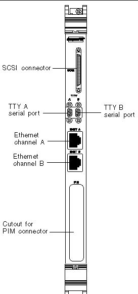
FIGURE A-1 shows the locations of the connectors on the Netra CP2140 host CPU board.
FIGURE A-1 Connectors on the Netra CP2140 Host CPU Board
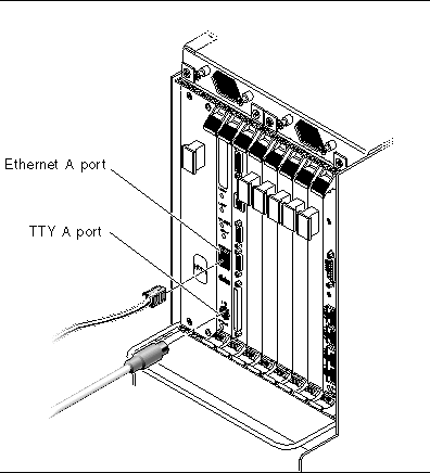
A.1.1.1 Ethernet A Port
The twisted pair Ethernet connector is an RJ-45 connector. The controller auto-negotiates to either 10BASE-T or 100/1000 BASE-T.
FIGURE A-2 RJ-45 Ethernet Connector Diagram
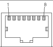
TABLE A-1 Ethernet Connector Pinouts, CPU Board (J2301)
|
Pin No.
|
Description
|
|
1
|
TXD+
|
|
2
|
TXD-
|
|
3
|
RXD+
|
|
4
|
4T_D3P
|
|
5
|
4T_D3P
|
|
6
|
RXD-
|
|
7
|
4T_D4P
|
|
8
|
4T_D4P
|
A.1.1.2 TTY A Port
This port is connected logically to serial port A. It is intended to be used only for serial output to a terminal.

|
Caution - Serial port A is connected through the rear cPCI connectors. No mechanism is provided to disable simultaneous input from the front panel and the rear cPCI connectors. Attempts to input data from both ports place the board in an unknown state.
|
FIGURE A-3 TTY A Connector
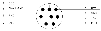
TABLE A-2 shows the TTY A connector pinouts.
TABLE A-2 TTY A Connector Pinouts
|
Pin
|
Signal Name
|
|
Pin
|
Signal Name
|
|
1
|
FP_SER_A_DTR
|
|
5
|
FP_SER_A_RXD
|
|
2
|
FP_SER_A_CTS
|
|
6
|
FP_SER_A_RTS
|
|
3
|
FP_SER_A_TXD
|
|
7
|
FP_SER_A_DCD
|
|
4
|
FP_SER_A_GND
|
|
8
|
Shield GND
|
A.1.2 Netra CP2500 Host CPU Board
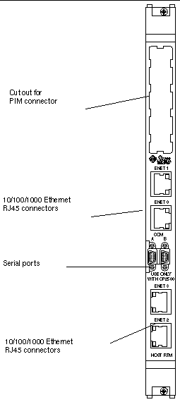
FIGURE A-4 shows the locations of the connectors on the Netra CP2500 host CPU board.
FIGURE A-4 Connectors on the Netra CP2500 Host CPU Board
A.1.2.1 PMC Connector
FIGURE A-5 and FIGURE A-6 show the location of PMC port connectors and pins. The following tables define contact allocations.
FIGURE A-5 Netra CP2500 Board PMC Port Connectors

|
Note - The P1386.1 standard reserves the Jn3 64-pin connector for PCI 64-bit extensions, so it is not fitted on the Netra CP2500 board.
|
FIGURE A-6 PMC Connector Slot Connector Pins

A.1.2.2 PMC Connector Interfaces
Corresponding to the Common Mezzanine Card (CMC) specification, the PMC A slot is comprised of three PMC connectors - Jn1, Jn2, and Jn4. (The Jn3 connector is not fitted on the Netra CP2500 board.)
|
Note - Sun does not support installing a PIM device on either the RTM-S or the RTM-H.
|
The following tables list the PMC slot connector interfaces.
TABLE A-3 PMC Jn1 Connector Interface
|
Pin
|
Description
|
Pin
|
Description
|
|
1
|
Not connected
|
2
|
-12V
|
|
3
|
GND
|
4
|
PMC_A_INT_A_L
|
|
5
|
PMC_A_INT_B_L
|
6
|
PMC_A_INT_C_L
|
|
7
|
PMC_BUSMODE1_L
|
8
|
VCC (5V)
|
|
9
|
PMC_A_INT_D_L
|
10
|
NC
|
|
11
|
GND
|
12
|
NC
|
|
13
|
PMC_CLK
|
14
|
GND
|
|
15
|
GND
|
16
|
PMC_GNT_L
|
|
17
|
PMC_REQ_L
|
18
|
VCC
|
|
19
|
LOCAL_VIO
|
20
|
PCI_B_AD<31>
|
|
21
|
PCI_B_AD<28>
|
22
|
PCI_B_AD<27>
|
|
23
|
PCI_B_AD<25>
|
24
|
GND
|
|
25
|
GND
|
26
|
PCI_B_CBE3_L
|
|
27
|
PCI_B_AD<22>
|
28
|
PCI_B_AD<21>
|
|
29
|
PCI_B_AD<19>
|
30
|
VCC
|
|
31
|
LOCAL_VIO
|
32
|
PCI_B_AD<17>
|
|
33
|
PCI_B_FRAME_L
|
34
|
GND
|
|
35
|
GND
|
36
|
PCI_B_IRDY_L
|
|
37
|
PCI_B_DEVSEL_L
|
38
|
VCC
|
|
39
|
GND
|
40
|
PCI_B_LOCK_L
|
|
41
|
PMC_SDONE
|
42
|
PMC_SB0_L
|
|
43
|
PCI_B_PAR
|
44
|
GND
|
|
45
|
LOCAL_VIO
|
46
|
PCI_B_AD<15>
|
|
47
|
PCI_B_AD<12>
|
48
|
PCI_B_AD<11>
|
|
49
|
PCI_B_AD<9>
|
50
|
VCC
|
|
51
|
GND
|
52
|
PCI_B_CBE_L<0>
|
|
53
|
PCI_B_AD<6>
|
54
|
PCI_B_AD<5>
|
|
55
|
PCI_B_AD<4>
|
56
|
GND
|
|
57
|
LOCAL_VIO
|
58
|
PCI_B_AD<3>
|
|
59
|
PCI_B_AD<2>
|
60
|
PCI_B_AD<1>
|
|
61
|
PCI_B_AD<0>
|
62
|
VCC
|
|
63
|
GND
|
64
|
PCI_B_REQ64_L
|
TABLE A-4 PMC Jn2 Connector Interface
|
Pin
|
Description
|
Pin
|
Description
|
|
1
|
+12V
|
2
|
JTAG_PMC_RST_L
|
|
3
|
TMS
|
4
|
PMC_TDO
|
|
5
|
PMC_TDI
|
6
|
GND
|
|
7
|
GND
|
8
|
NC
|
|
9
|
NC
|
10
|
NC
|
|
11
|
PMC_BUSMODE2_L
|
12
|
VDD (3.3V)
|
|
13
|
PCI_B_RST_L
|
14
|
PMC_BUSMODE3_L
|
|
15
|
VDD
|
16
|
PMC_BUSMODE4_L
|
|
17
|
NC
|
18
|
GND
|
|
19
|
PCI_B_AD<30>
|
20
|
PCI_B_AD<29>
|
|
21
|
GND
|
22
|
PCI_B_AD<26>
|
|
23
|
PCI_B_AD<24>
|
24
|
VDD
|
|
25
|
PCI_B_IDSEL
|
26
|
PCI_B_AD<23>
|
|
27
|
VDD
|
28
|
PCI_B_AD<20>
|
|
29
|
PCI_B_AD<18>
|
30
|
GND
|
|
31
|
PCI_B_AD<16>
|
32
|
PCI_B_CBE_L<2>
|
|
33
|
GND
|
34
|
NC
|
|
35
|
PCI_B_TRDY_L
|
36
|
VDD
|
|
37
|
GND
|
38
|
PCI_B_STOP_L
|
|
39
|
PCI_B_PERR_L
|
40
|
GND
|
|
41
|
VDD
|
42
|
PCI_B_SERR_L
|
|
43
|
PCI_B_CBE_L<1>
|
44
|
GND
|
|
45
|
PCI_B_AD<14>
|
46
|
PCI_B_AD<13>
|
|
47
|
GND
|
48
|
PCI_B_AD<10>
|
|
49
|
PCI_B_AD<8>
|
50
|
VDD
|
|
51
|
PCI_B_AD<7>
|
52
|
NC
|
|
53
|
VDD
|
54
|
NC
|
|
55
|
NC
|
56
|
GND
|
|
57
|
NC
|
58
|
NC
|
|
59
|
GND
|
60
|
NC
|
|
61
|
PCI_B_ACK64_L
|
62
|
VDD
|
|
63
|
GND
|
64
|
NC
|
|
Note - The P1386.1 standard reserves the Jn3 64-pin connector for PCI 64-bit extensions. It is not fitted on these boards.
|
TABLE A-5 PMC Jn4 Connector Interface
|
Pin
|
Description
|
Pin
|
Description
|
|
1
|
Not connected
|
2
|
Not connected
|
|
3
|
Not connected
|
4
|
Not connected
|
|
5
|
Not connected
|
6
|
Not connected
|
|
7
|
Not connected
|
8
|
Not connected
|
|
9
|
Not connected
|
10
|
Not connected
|
|
11
|
Not connected
|
12
|
Not connected
|
|
13
|
Not connected
|
14
|
Not connected
|
|
15
|
Not connected
|
16
|
Not connected
|
|
17
|
Not connected
|
18
|
Not connected
|
|
19
|
Not connected
|
20
|
Not connected
|
|
21
|
Not connected
|
22
|
Not connected
|
|
23
|
Not connected
|
24
|
Not connected
|
|
25
|
Not connected
|
26
|
Not connected
|
|
27
|
Not connected
|
28
|
Not connected
|
|
29
|
Not connected
|
30
|
Not connected
|
|
31
|
Not connected
|
32
|
Not connected
|
|
33
|
PMC_A_IO_33
|
34
|
PMC_A_IO_34
|
|
35
|
PMC_A_IO_35
|
36
|
PMC_A_IO_36
|
|
37
|
PMC_A_IO_37
|
38
|
PMC_A_IO_38
|
|
39
|
PMC_A_IO_39
|
40
|
PMC_A_IO_40
|
|
41
|
PMC_A_IO_41
|
42
|
PMC_A_IO_42
|
|
43
|
PMC_A_IO_43
|
44
|
PMC_A_IO_44
|
|
45
|
PMC_A_IO_45
|
46
|
PMC_A_IO_46
|
|
47
|
PMC_A_IO_47
|
48
|
PMC_A_IO_48
|
|
49
|
Not connected
|
50
|
Not connected
|
|
51
|
Not connected
|
52
|
Not connected
|
|
53
|
Not connected
|
54
|
Not connected
|
|
55
|
Not connected
|
56
|
Not connected
|
|
57
|
Not connected
|
58
|
Not connected
|
|
59
|
Not connected
|
60
|
Not connected
|
|
61
|
Not connected
|
62
|
Not connected
|
|
63
|
Not connected
|
64
|
Not connected
|
A.1.2.3 Front Panel Serial Connector
This section contains the pin assignments for the front panel serial port connector.
FIGURE A-7 Front Panel Serial Port Diagram

TABLE A-2 shows the serial port connector (TTYA) pin assignments.
TABLE A-6 Serial Micro DB9 Connector Pinouts
|
Pin
|
Signal Name
|
Pin
|
Signal Name
|
|
1
|
SER_DCD
|
6
|
SER_OSR
|
|
2
|
SER_RXD
|
7
|
SER_RTS
|
|
3
|
SER_TXD
|
8
|
SER_CTS
|
|
4
|
SER_DTR
|
9
|
SER_RI
|
|
5
|
SER_GND
|
|
|
A.1.2.4 Backplane Connectors
FIGURE A-8 shows contact numbering as seen from the back of the Netra CT board.
FIGURE A-8 Backplane Connector Contact Numbering

|
Note - The CompactPCI J4 connector is not populated on the Netra CP2500 board.
|
A.1.2.5 CompactPCI J1/P1 Connector Pinouts
TABLE A-7 lists the CompactPCI J1/P1 connector pin assignments.
TABLE A-7 CompactPCI J2/P2 Connector Pin Assignments
|
Pin
|
Row Z
|
Row A
|
Row B
|
Row C
|
Row D
|
Row E
|
Row F
|
|
25
|
GND
|
+EP_5V
|
CPCI_REQ64#
|
CPCI_ENUM#
|
+EP_3.3V
|
+EP_5V
|
GND
|
|
24
|
GND
|
CPCI_AD[1]
|
+EP_5V
|
LP_VIO/unused
|
CPCI_AD[0]
|
CPCI_ACK64#
|
GND
|
|
23
|
GND
|
+EP_3.3V
|
CPCI_AD[4]
|
CPCI_AD[3]
|
LP_+EP_5V
|
CPCI_AD[2]
|
GND
|
|
22
|
GND
|
CPCI_AD[7]
|
GND
|
LP_+EP_3.3V
|
CPCI_AD[6]
|
CPCI_AD[5]
|
GND
|
|
21
|
GND
|
+EP_3.3V
|
CPCI_AD[9]
|
CPCI_AD[8]
|
m66en
|
CPCI_C/BE[0]#
|
GND
|
|
20
|
GND
|
CPCI_AD[12]
|
GND
|
VIO (+EP_SV)
|
CPCI_AD[11]
|
CPCI_AD[10]
|
GND
|
|
19
|
GND
|
+EP_3.3V
|
CPCI_AD[15]
|
CPCI_AD[14]
|
LP_GND
|
CPCI_AD[13]
|
GND
|
|
18
|
GND
|
CPCI_SERR#
|
GND
|
+EP_3.3V
|
CPCI_PAR
|
CPCI_C/BE[1]#
|
GND
|
|
17
|
GND
|
+EP_3.3V
|
IPMB_SCL
|
IPMB_SDA
|
LP_GND
|
CPCI_PERR#
|
GND
|
|
16
|
GND
|
CPCI_DEVSL#
|
GND
|
VIO* (+EP_SV)
|
CPCI_STOP#
|
lock#
|
GND
|
|
15
|
GND
|
+EP_3.3V
|
CPCI_FRAME#
|
CPCI_IRDY#
|
CPCI_BD_SEL#
|
CPCI_TRDY#
|
GND
|
|
14
|
Key
|
|
|
|
|
|
Key
|
|
13
|
Key
|
|
|
|
|
|
Key
|
|
12
|
Key
|
|
|
|
|
|
Key
|
|
11
|
GND
|
CPCI_AD[18]
|
CPCI_AD[17]
|
CPCI_AD[16]
|
LP_GND
|
CPCI_C/BE[2]#
|
GND
|
|
10
|
GND
|
CPCI_AD[21]
|
GND
|
+EP_3.3V
|
CPCI_AD[20]
|
CPCI_AD[19]
|
GND
|
|
9
|
GND
|
CPCI_C/BE[3]#
|
CPCI_IDSEL
|
CPCI_AD[23]
|
LP_GND
|
CPCI_AD[22]
|
GND
|
|
8
|
GND
|
CPCI_AD[26]
|
GND
|
VIO* (+EP_SV)
|
CPCI_AD[25]
|
CPCI_AD[24]
|
GND
|
|
7
|
GND
|
CPCI_AD[30]
|
CPCI_AD[29]
|
CPCI_AD[28]
|
LP_GND
|
CPCI_AD[27]
|
GND
|
|
6
|
GND
|
CPCI_REQ0#
|
PCI_PRES#
|
LP_+EP_3.3V
|
CPCI_CLK0
|
CPCI_AD[31]
|
GND
|
|
5
|
GND
|
BRSVP
|
BRSVP
|
CPCI_RST#
|
LP_GND
|
CPCI_GNT0#
|
GND
|
|
4
|
GND
|
IPMB_PWR
|
HEALTHY#_out
|
LP_VIO/unused
|
intp
|
ints
|
GND
|
|
3
|
GND
|
CPCI_INTA#
|
CPCI_INTB#
|
CPCI_INTC#
|
LP_+EP_5V
|
CPCI_INTD#
|
GND
|
|
2
|
GND
|
tck
|
+EP_5V
|
tms
|
tdo
|
tdi
|
GND
|
|
1
|
GND
|
+EP_5V
|
-EP_12V
|
trst#
|
+EP_12V
|
+EP_5V
|
GND
|
A.1.2.6 CompactPCI J1/P1 Signal Descriptions

|
Caution - Backplane power input (VIO) mustbe 5V.
|
TABLE A-8 CompactPCI J1/P1 Signal Descriptions
|
Signal Name
|
Description
|
|
+EP_5V
|
Backplane power input, EP_5V.
|
|
+EP_3.3V
|
Backplane power input, EP_3.3V.
|
|
+EP_12V
|
Backplane power input, EP_12V.
|
|
-EP_12V
|
Backplane power input, -EP_12V.
|
|
VIO
|
Backplane power input, which must be EP_5V.
|
|
LP_*
|
Long power pins. Refer to the PCIMG Hot Swap Spec R2.0, Section 4.2.1.
|
|
CPCI_RST#
|
cPCI reset.
|
|
CPCI_CLK[7..0]
|
cPCI clock. Provides timing for all cPCI transactions.
|
|
CPCI_AD[63..0]
|
cPCI bus Interface 64-bit multiplexed address and data.
|
|
CPCI_C/BE[7..0]#
|
cPCI bus command and byte enables; multiplexed on the same PCI signals.
|
|
CPCI_FRAME#
|
cPCI frame. Indicates the beginning of a PCI bus cycle.
|
|
CPCI_DEVSEL#
|
cPCI device select. Indicates PCI device response to selection.
|
|
CPCI_IRDY#
|
cPCI initiator ready. indicate bus master ability to complete the current data phase.
|
|
CPCI_TRDY#
|
cPCI target ready. Indicates target ability to complete the current data phase.
|
|
CPCI_STOP#
|
cPCI stop. Indicates initiator or target is requesting to stop the current transaction.
|
|
CPCI_IDSEL
|
cPCI initialization device select. Chip select during configuration read and write.
|
|
CPCI_REQ64#
|
cPCI request 64-bit transfer.
|
|
CPCI_ACK64#
|
cPCI Acknowledge 64-bit Transfer.
|
|
CPCI_PAR
|
cPCI parity bit. Calculated across AD[31..0] and C/BE[3..0].
|
|
CPCI_PERR#
|
Parity error.
|
|
CPCI_SERR#
|
cPCI system error.
|
|
CPCI_INT[A-D]
|
cPCI interrupts.
|
|
CPCI_REQ[7..0]#
|
cPCI request. Indicates to arbiter an agent desires use of the cPCI bus.
|
|
CPCI_GNT[7..0]#
|
cPCI grant. Indicates to agent access to the bus has been granted.
|
|
CPCI_BD_SEL#
|
PICMG 2.1 R1.0 hot-swap signal. Indicate board presence, SC drives to power on.
|
|
CPCI_ENUM#
|
PICMG 2.1 R1.0 hot-swap signal. Send or receive insertion or extraction event.
|
|
HEALTHY#_out
|
PICMG 2.1 R1.0 hot-swap signal. Indicates health of the board, and signals to the SC that the board is suitable to be released from reset and enabled onto the bus.
|
|
IPMB_SCL
|
IPMI bus clock signal. Refer to the PCIMG 2.9 R1.0 cPCI System Management document.
|
|
IPMB_SDA
|
IPMI bus data signal. Refer to the PCIMG 2.9 R1.0 cPCI System Management document.
|
|
IPMB_PWR
|
Back-up power signal. Refer to the PCIMG 2.9 R1.0 cPCI System Management document.
|
|
PCI_PRES#
|
Indicates the backplane slot supports the cPCI interface.
|
|
m66en
|
66MHz cPCI bus speed enable; not supported.
|
|
lock#
|
cPCI Lock; not supported.
|
|
intp
|
Non-cPCI Interrupt; not supported.
|
|
ints
|
Non-cPCI Interrupt; not supported.
|
|
tck, tms, tdo, tdi
|
JTAG Signals; not supported, unconnected.
|
|
BRSVP
|
Backplane bused reserve pins, unconnected.
|
A.1.2.7 CompactPCI J2/P2 Connector Pinouts
TABLE A-9 lists the CompactPCI J2 connector pin assignments.
TABLE A-9 CompactPCI J2/P2 Connector Pin Assignments
|
Pin
|
Row Z
|
Row A
|
Row B
|
Row C
|
Row D
|
Row E
|
Row F
|
|
22
|
GND
|
CPCI_GA4
|
CPCI_GA3
|
CPCI_GA2
|
CPCI_GA1
|
CPCI_GA0
|
GND
|
|
21
|
GND
|
CPCI_CLK6
|
GND
|
RSV
|
RSV
|
rsv
|
GND
|
|
20
|
GND
|
CPCI_CLK5
|
GND
|
rsv
|
GND
|
rsv
|
GND
|
|
19
|
GND
|
GND
|
GND
|
rsv
|
rsv
|
rsv
|
GND
|
|
18
|
GND
|
BRSVP
|
BRSVP
|
BRSVP
|
GND
|
BRSVP
|
GND
|
|
17
|
GND
|
BRSVP
|
GND
|
BP_PB_RST#
|
CPCI_REQ6#
|
CPCI_GNT6#
|
GND
|
|
16
|
GND
|
BRSVP
|
BRSVP
|
DEG#
|
GND
|
BRSVP
|
GND
|
|
15
|
GND
|
BRSVP
|
GND
|
FAL#
|
CPCI_REQ5#
|
CPCI_GNT5#
|
GND
|
|
14
|
GND
|
CPCI_AD[35]
|
CPCI_AD[34]
|
CPCI_AD[33]
|
GND
|
CPCI_AD[32]
|
GND
|
|
13
|
GND
|
CPCI_AD[38]
|
GND
|
VIO/unused
|
CPCI_AD[37]
|
CPCI_AD[36]
|
GND
|
|
12
|
GND
|
CPCI_AD[42]
|
CPCI_AD[41]
|
CPCI_AD[40]
|
GND
|
CPCI_AD[39]
|
GND
|
|
11
|
GND
|
CPCI_AD[45]
|
GND
|
VIO/unused
|
CPCI_AD[44]
|
CPCI_AD[43]
|
GND
|
|
10
|
GND
|
CPCI_AD[49]
|
CPCI_AD[48]
|
CPCI_AD[47]
|
GND
|
CPCI_AD[46]
|
GND
|
|
9
|
GND
|
CPCI_AD[52]
|
GND
|
VIO (+EP_5V)
|
CPCI_AD[51]
|
CPCI_AD[50]
|
GND
|
|
8
|
GND
|
CPCI_AD[56]
|
CPCI_AD[55]
|
CPCI_AD[54]
|
GND
|
CPCI_AD[53]
|
GND
|
|
7
|
GND
|
CPCI_AD[59]
|
GND
|
VIO* (+EP_5V)
|
CPCI_AD[58]
|
CPCI_AD[57]
|
GND
|
|
6
|
GND
|
CPCI_AD[63]
|
CPCI_AD[62]
|
CPCI_AD[61]
|
GND
|
CPCI_AD[60]
|
GND
|
|
5
|
GND
|
CPCI_C/BE[5]#
|
CPCI_64_EN#
|
VIO* (+EP_5V)
|
CPCI_C/BE[4]#
|
CPCI_PAR64
|
GND
|
|
4
|
GND
|
rsv
|
BRSVP
|
CPCI_C/BE[7]#
|
GND
|
CPCI_C/BE[6]#
|
GND
|
|
3
|
GND
|
CPCI_CLK4
|
GND
|
CPCI_GNT3#
|
CPCI_REQ4#
|
CPCI_GNT4#
|
GND
|
|
2
|
GND
|
CPCI_CLK2
|
CPCI_CLK3
|
CPCI_SYSEN#
|
CPCI_GNT2#
|
CPCI_REQ3#
|
GND
|
|
1
|
GND
|
CPCI_CLK1
|
GND
|
CPCI_REQ1#
|
CPCI_GNT1#
|
CPCI_REQ2#
|
GND
|
A.1.2.8 CompactPCI J2/P2 Signal Descriptions

|
Caution - Select VIO pins mustbe set to 5V, and notto universal.
|
TABLE A-10 CompactPCI J2/P2 Signal Descriptions
|
Signal Name
|
Description
|
|
CPCI_GA[4..0]
|
Geographical Address. Signals for unique slot identification.
|
|
BRSVP
|
Bused reserve pins.
|
|
PRST#
|
Backplane button reset input to SMC.
|
|
DEG#, FAL#
|
Power subsystem status signals input to SMC.
|
|
CPCI_64_EN#
|
PICMG hot-swap spec 2.1 R1.0 signal; designates 64-bit capability of backplane slot.
|
|
CPCI_PAR64
|
cPCI parity 64 bit; calculated across AD[63..32] and C/ BE[7..4]#.
|
|
CPCI_SYSEN#
|
System slot identification, grounded on the cPCI system slot.
|
A.1.2.9 CompactPCI J3/P3 Connector Pinouts
TABLE A-11 lists the CompactPCI J3 connector pin assignments.
TABLE A-11 CompactPCI J3/P3 Connector Pin Assignments
|
Pin
|
Row Z
|
Row A
|
Row B
|
Row C
|
Row D
|
Row E
|
Row F
|
|
19
|
GND
|
RTM GND
|
RTM GND
|
RTM GND
|
RTM GND
|
RTM GND
|
GND
|
|
18
|
GND
|
PSB_A_TX_POS
|
PSB_A_TX_NEG
|
GND
|
GbE_A_TX_POS
|
GbE_A_TX_NEG
|
GND
|
|
17
|
GND
|
PSB_A_RX_POS
|
PSB_A_RX_NEG
|
GND
|
GbE_A_RX_POS
|
GbE_A_RX_NEG
|
GND
|
|
16
|
GND
|
PSB_B_TX_POS
|
PSB_B_TX_NEG
|
GND
|
GbE_B_TX_POS
|
GbE_B_TX_NEG
|
GND
|
|
15
|
GND
|
PSB_B_RX_POS
|
PSB_B_RX_NEG
|
GND
|
GbE_B_RX_POS
|
GbE_B_RX_NEG
|
GND
|
|
14
|
GND
|
RTM +3.3V
|
RTM +3.3V
|
RTM +3.3V
|
RTM +3.3V
|
RTM +3.3V
|
GND
|
|
13
|
GND
|
PCI A AD[31]
|
PCI A AD[30]
|
PCI A AD[29]
|
PCI A AD[28]
|
PCI A AD[27]
|
GND
|
|
12
|
GND
|
PCI A AD[26]
|
PCI A AD[25]
|
PCI A AD[24]
|
PCI A AD[23]
|
PCI A AD[22]
|
GND
|
|
11
|
GND
|
PCI A AD[21]
|
PCI A AD[20]
|
PCI A AD[19]
|
PCI A AD[18]
|
PCI A AD[17]
|
GND
|
|
10
|
GND
|
PCI A AD[16]
|
PCI A AD[15]
|
PCI A AD[14]
|
PCI A AD[13]
|
PCI A AD[12]
|
GND
|
|
9
|
GND
|
PCI A AD[11]
|
PCI A AD[10]
|
PCI A AD[9]
|
PCI A AD[8]
|
PCI A AD[7]
|
GND
|
|
8
|
GND
|
PCI A AD[6]
|
PCI A AD[5]
|
PCI A AD[4]
|
PCI A AD[3]
|
PCI A AD[2]
|
GND
|
|
7
|
GND
|
PCI A AD[1]
|
PCI A AD[0]
|
PCI A FRAM#
|
PCI A DVSL#
|
PCI A IRDY#
|
GND
|
|
6
|
GND
|
PCI A CBE0#
|
healthy_BP_RSV
|
PCI A CBE1#
|
PCI A TRDY#
|
PCI A STOP#
|
GND
|
|
5
|
GND
|
RTM SCA INT#
|
healthy_BP_RSV
|
RTM NTB INT#
|
PCI A PAR
|
PCI A CBE3#
|
GND
|
|
4
|
GND
|
RTM SCB INT#
|
healthy_BP_RSV
|
RTM NTA INT#
|
PCI A CBE2#
|
PCI A RTM CLKB
|
GND
|
|
3
|
GND
|
PCI A GNT 1#
|
healthy_BP_RSV
|
PCI A REQ1#
|
PCI A RST#
|
PCI A SERR#
|
GND
|
|
2
|
GND
|
PCI A GNT 2#
|
healthy_BP_RSV
|
PCI A REQ2#
|
SMC_3P3V
|
healthy_BP_RSV
|
GND
|
|
1
|
GND
|
Vdd 2.5V
|
healthy_BP_RSV
|
PCI A 66EN
|
PCI A RTM CLKA
|
PCI A PERR#
|
GND
|
A.1.2.10 CompactPCI J3/P3 Signal Descriptions
TABLE A-12 CompactPCI J3/P3 Signal Descriptions
|
Signal Name
|
Description
|
|
GbE/PSB_TX/RX_POS/NEG
|
PICMG 2.16 node board 10/100/1000 network signals.
|
|
32-bit PCI bus
|
32-bit PCI bus signaling and additional power pins to support SCSI controller on RTM-H. Optional.
|
A.1.2.11 CompactPCI J5/P5 Connector Pinouts
TABLE A-13 lists the CompactPCI J5 connector pin assignments.
TABLE A-13 CompactPCI J5/P5 Connector Pin Assignments
|
Pin
|
Row Z
|
Row A
|
Row B
|
Row C
|
Row D
|
Row E
|
Row F
|
|
22
|
GND
|
RSV
|
GND
|
No Connect
|
+5V
|
BP_XIR#
|
GND
|
|
21
|
GND
|
P1 LINKLED#
|
P1 ACTLED#
|
P2 LINKLED#
|
RTM I2C SCL
|
P2 ACTLED#
|
GND
|
|
20
|
GND
|
+5V
|
RSV
|
RSV
|
RTM I2C SDA
|
+12V
|
GND
|
|
19
|
GND
|
RSV
|
GND
|
VCC
|
SMC PWR
|
-12V
|
GND
|
|
18
|
GND
|
RSV
|
RSV
|
RSV
|
GND
|
+5V
|
GND
|
|
17
|
GND
|
RSV
|
RSV
|
RSV
|
RSV
|
RSV
|
GND
|
|
16
|
GND
|
RSV
|
RSV
|
RSV
|
RSV
|
RSV
|
GND
|
|
15
|
GND
|
RSV
|
RSV
|
RSV
|
RSV
|
RSV
|
GND
|
|
14
|
GND
|
RTSA
|
CTSA
|
RIA
|
GND
|
DTRA
|
GND
|
|
13
|
GND
|
DCDA
|
+5V
|
RXDA
|
DSRA
|
TXDA
|
GND
|
|
12
|
GND
|
RTSB
|
CTSB
|
RIB
|
+5V
|
DTRB
|
GND
|
|
11
|
GND
|
DCDB
|
GND
|
RXDB
|
DSRB
|
TXDB
|
GND
|
|
10
|
GND
|
PMC IO[36]
|
PMC IO[45]
|
PMC IO[47]
|
PMC IO[46]
|
PMC IO[48]
|
GND
|
|
9
|
GND
|
PMC IO[34]
|
PMC IO[41]
|
PMC IO[43]
|
PMC IO[42]
|
PMC IO[44]
|
GND
|
|
8
|
GND
|
PMC IO[35]
|
PMC IO[37]
|
PMC IO[39]
|
PMC IO[38]
|
PMC IO[40]
|
GND
|
|
7
|
GND
|
PMC IO[33]
|
RSV
|
RSV
|
RSV
|
RSV
|
GND
|
|
6
|
GND
|
RSV
|
GND
|
RSV
|
RSV
|
RSV
|
GND
|
|
5
|
GND
|
RSV
|
RSV
|
RSV
|
RSV
|
RSV
|
GND
|
|
4
|
GND
|
RSV
|
RSV
|
GND
|
RSV
|
RSV
|
GND
|
|
3
|
GND
|
RSV
|
RSV
|
RSV
|
RSV
|
RSV
|
GND
|
|
2
|
GND
|
RSV
|
RSV
|
RSV
|
RSV
|
RSV
|
GND
|
|
1
|
GND
|
RSV
|
RSV
|
RSV
|
RSV
|
RSV
|
GND
|
A.1.2.12 CompactPCI J5/P5 Signal Descriptions
TABLE A-14 lists the serial COM port (A and B) and RS232 level signal descriptions.
TABLE A-14 Serial COM Port and RS232 Level CompactPCI J5/P5 Signal Descriptions
|
Pin Signal
|
Description
|
|
CTS
|
Clear to send.
|
|
DCD
|
Data carrier detected.
|
|
DSR
|
Data set ready.
|
|
DTR
|
Data terminal ready.
|
|
RI
|
Ring indicator.
|
|
RTS
|
Request to send.
|
|
RXD
|
Serial receive data.
|
|
TXD
|
Serial transmit data.
|
FIGURE A-9 lists the miscellaneous signal descriptions.
TABLE A-15 Miscellaneous CompactPCI J5/P5 Signal Descriptions
|
Pin Signal
|
Description
|
|
BP_XIR_L
|
Button reset system input. Active low.
|
A.1.2.13 DIP Switch Settings
The Netra CP2500 board contains two DIP switches on one bank. The SW3301 DIP switch bank is located on the component side of the board between the front panel and heat sink (see FIGURE A-9). TABLE A-16 describes these switch settings.
FIGURE A-9 SW3301 DIP Switch Location

|
Note - By default, the SW3301 DIP switches are both set in an open position, which means they are set in the opposite direction of the arrow. FIGURE A-9 shows the two switches in the default, open position.
|
TABLE A-16 SW3301 Switch Descriptions
|
Switch
|
Switch Setting
|
Description
|
|
1
|
Open
|
Boot the board from the main OpenBoot PROM image (default setting)
|
|
|
Closed
|
Boot the board from the backup OpenBoot PROM image in the system flash
|
|
2
|
Open
|
Board is set to operate in a cPCI server (default setting)
|
|
|
Closed
|
Board is set to operate in a cPSB chassis
|
|
Note - When switch 2 is set to the closed position (the cPSB chassis setting), the board's cPCI bridge will not be taken out of reset.
|
|
Note - The Netra CP2500 board is only supported in a Netra CT 410 server, Netra CT 810 server, or a third-party cPSB chassis. Sun does not support operating the Netra CP2500 board in a third-party cPCI server.
|
A.2 Host Rear Transition Modules
The following are possible host board and rear transition module combinations:
- Netra CP2140 and Netra CPU transition card (CTC, hereafter referred to as rear transition module)
- Netra CP2500 and Netra CP2500 RTM-H (rear transition module-host)
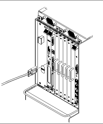
A.2.1 Netra CP2140 Host RTMs
FIGURE A-10 shows the locations of the connectors on the Netra CP2140 rear transition module. When using the Netra CP2140 host board, the RTM is the same for both the Netra CT 810 server and the Netra CT 410; only the location in the rear board cage differs.
FIGURE A-10 Connectors on the Netra CP2140 Rear Transition Module
A.2.1.1 SCSI (VHDC)
The SCSI port on the CPU RTM is a 68-pin CHAMP very high density connector (VHDC). A VHDC-to-SCSI 3 cable is available through Sun, if necessary (part number 530-2453-xx, X3832A).
TABLE A-17 SCSI Port Pinouts, CPU RTC
|
Pin No.
|
Signal
|
|
Pin No.
|
Signal
|
|
Pin No.
|
Signal
|
|
1
|
GND
|
|
24
|
GND
|
|
47
|
DATA 7
|
|
2
|
PRES_L
|
|
25
|
GND
|
|
48
|
PL_L
|
|
3
|
GND
|
|
26
|
GND
|
|
49
|
PRES_L
|
|
4
|
GND
|
|
27
|
GND
|
|
50
|
GND
|
|
5
|
GND
|
|
28
|
GND
|
|
51
|
TERM PWR
|
|
6
|
GND
|
|
29
|
GND
|
|
52
|
TERM PWR
|
|
7
|
GND
|
|
30
|
GND
|
|
53
|
GND
|
|
8
|
GND
|
|
31
|
GND
|
|
54
|
GND
|
|
9
|
GND
|
|
32
|
GND
|
|
55
|
ATN_L
|
|
10
|
GND
|
|
33
|
GND
|
|
56
|
GND
|
|
11
|
GND
|
|
34
|
GND
|
|
57
|
BSY_L
|
|
12
|
GND
|
|
35
|
DATA 12
|
|
58
|
ACK_L
|
|
13
|
GND
|
|
36
|
DATA 13
|
|
59
|
RST_L
|
|
14
|
GND
|
|
37
|
DATA 14
|
|
60
|
MSG_L
|
|
15
|
GND
|
|
38
|
DATA 15
|
|
61
|
DEL_L
|
|
16
|
GND
|
|
39
|
PH_L
|
|
62
|
CD_L
|
|
17
|
TERM PWR
|
|
40
|
DATA 0
|
|
63
|
REQ_L
|
|
18
|
TERM PWR
|
|
41
|
DATA 1
|
|
64
|
IO_L
|
|
19
|
GND
|
|
42
|
DATA 2
|
|
65
|
DATA 8
|
|
20
|
GND
|
|
43
|
DATA 3
|
|
66
|
DATA 9
|
|
21
|
GND
|
|
44
|
DATA 4
|
|
67
|
DATA 10
|
|
22
|
GND
|
|
45
|
DATA 5
|
|
68
|
DATA 11
|
|
23
|
GND
|
|
46
|
DATA 6
|
|
|
|
A.2.1.2 TTY A and B Ports
The TTY A and B ports are stacked mini 9-pin connectors. The signal interface of the connector is as follows.
TABLE A-18 Signal Interfaces for TTY A and B Port Connectors
|
TTY A of Dual Connector
|
|
TTY B of Dual Connector
|
|
Pin
|
Signal
|
|
Pin
|
Signal
|
|
P1A
|
DCDA
|
|
P1B
|
DCDB
|
|
P2A
|
RXDA
|
|
P2B
|
RXDB
|
|
P3A
|
TXDA
|
|
P3B
|
TXDB
|
|
P4A
|
DTRA
|
|
P4B
|
DTRB
|
|
P5A
|
DGNDA
|
|
P5B
|
DGNDB
|
|
P6A
|
DSRA
|
|
P6B
|
DSRB
|
|
P7A
|
RTSA
|
|
P7B
|
RTSB
|
|
P8A
|
CTSA
|
|
P8B
|
CTSB
|
|
P9A
|
RIA
|
|
P9B
|
RIB
|
|
Note - The two TTY ports require the use of specific adapter cables. Use the Serial Cable Adapter, MDSM-9F to DB9M, (6 inch, 9 wires), P/N C-CEL-10110-10. The manufacturer is Computer Cable Makers Inc. and cables can be ordered directly from the manufacturer.
|
A.2.1.3 Ethernet A and B Ports
The Ethernet A and B ports on the CPU RTC are RJ-45 connectors for 10/100 Mbps.
FIGURE A-11 RJ-45 Ethernet Connector Diagram

TABLE A-19 Ethernet A and B Connector Pinouts, CPU RTM
|
Pin No.
|
Description
|
|
1
|
TXD+
|
|
2
|
TXD-
|
|
3
|
RXD+
|
|
4
|
Not used
|
|
5
|
Not used
|
|
6
|
RXD-
|
|
7
|
Not used
|
|
8
|
Not used
|
A.2.1.4 PIM Module Interface
The host CPU rear transition module supports a PCI mezzanine card (PMC) I/O module (PIM). A PIM is generally located on a rear transition module to enable rear I/O from the CompactPCI bus chassis. Custom PIMs provide additional I/Os that do not fit on the standard rear transition module rear panel. (For more information on PIM slot mechanics, electrical and logical information, refer to VITA 36 - PMC I/O Module Standard available http://www.vita.com and the IEEE P1386 Standard). The single-sized PIM measures 2.92 inches (74 mm) wide and 2.72 inches (69 mm) deep.
The PIM module must be mounted on the host CPU rear transition module before the rear transition module is inserted in a Netra CT server.

|
Caution - A PIM module must be used with its matching PMC. Any other combination could lead to damage of the PIM or PMC.
|
A.2.2 Netra CP2500 Host RTMs
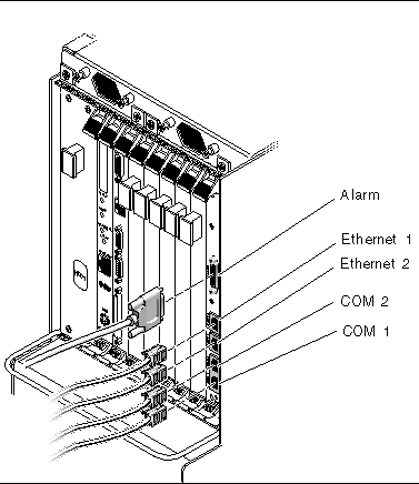
FIGURE A-12 shows connectors on the Netra CP2500 host rear transistion module (RTM-H). When using the Netra CP2500 host board, the RTM-H is the same for both the Netra CT 810 server and the Netra CT 410; only the location in the rear board cage differs.
FIGURE A-12 Connectors on the Netra CP2500 Rear Transition Module-Host (RTM-H)
A.2.2.1 Serial Ports
Two serial ports from the Netra CP2500 transition module are available through the rear panel with single-stacked, 9-pin connectors. One connector is assigned to Port A and the other connector to Port B (FIGURE A-13).
FIGURE A-13 Serial Port Connector Pins

The signal interface of the connectors are described in the following two tables.
TABLE A-20 Serial Port A
|
Pin
|
Signal
|
|
1
|
SER_A_DCD
|
|
2
|
SER_A_RXD
|
|
3
|
SER_A_TXD
|
|
4
|
SER_A_DTR
|
|
5
|
GND_A
|
|
6
|
SER_A_DSR
|
|
7
|
SER_A_RTS
|
|
8
|
SER_A_CTS
|
|
9
|
SER_A_RI
|
TABLE A-21 Serial Port B
|
Pin
|
Signal
|
|
1
|
SER_B_DCD
|
|
2
|
SER_B_RXD
|
|
3
|
SER_B_TXD
|
|
4
|
SER_B_DTR
|
|
5
|
GND_B
|
|
6
|
SER_B_DSR
|
|
7
|
SER_B_RTS
|
|
8
|
SER_B_CTS
|
|
9
|
SER_B_RI
|
A.2.2.2 Ethernet Connectors
Two single-jack RJ45 XFMRS XFGIB look-CLYGI-4MS Ethernet connectors and two single-jack RJ45 Amphenol RJH55381 Ethernet conectors located on the transition module's back panel, provide two 10/100/1000 Mbps Ethernet ports.
FIGURE A-14 Ethernet Port Connector Pins

Ethernet ports, ENET0 and ENET1 are not available if the Netra CP2500 board is set to use the chassis's packet-switched backplane (PSB) Ethernet network. In order to use the transition module's Ethernet connectors, you must set the S1301 and S1302 switches to the On position (see FIGURE A-16), which is their default position.
TABLE A-22 lists the pin assignments for the two RJ45 XFMRS XFGIB look-CLYGI-4MS Ethernet connectors.
TABLE A-22 ENET0 and ENET1
|
ENET0
|
ENET1
|
|
Pin
|
Signal
|
Pin
|
Signal
|
|
1
|
TRDP0
|
1
|
TRDP0
|
|
2
|
TRDN0
|
2
|
TRDN0
|
|
3
|
TRDP1
|
3
|
TRDP1
|
|
4
|
TRDP2
|
4
|
TRDP2
|
|
5
|
TRDN2
|
5
|
TRDN2
|
|
6
|
TRDN1
|
6
|
TRDN1
|
|
7
|
TRDP3
|
7
|
TRDP3
|
|
8
|
TRDN3
|
8
|
TRDN3
|
TABLE A-23 lists the pin assignments for the two single-jack RJ45 Amphenol RJH55381 Ethernet conectors.
TABLE A-23 ENET2 and ENET3
|
ENET3
|
ENET4
|
|
Pin
|
Signal
|
Pin
|
Signal
|
|
1
|
TRDP0
|
1
|
TRDP0
|
|
2
|
TRDN0
|
2
|
TRDN0
|
|
3
|
TRDP1
|
3
|
TRDP1
|
|
4
|
TRDP2
|
4
|
TRDP2
|
|
5
|
TRDN2
|
5
|
TRDN2
|
|
6
|
TRDN1
|
6
|
TRDN1
|
|
7
|
TRDP3
|
7
|
TRDP3
|
|
8
|
TRDN3
|
8
|
TRDN3
|
A.2.2.3 On-Board Interfaces and Connectors on the Netra CP2500 Transition Module
FIGURE A-15 shows the on-board interfaces and connectors on the RTM-H. FIGURE A-16 shows the on-board interfaces and connectors on the RTM-S. The numbers in parentheses display how the interfaces are labeled on the transition module.
FIGURE A-15 On-Board Connectors and Interfaces for the Netra CP2500 RTM-H

FIGURE A-16 On-Board Connectors and Interfaces for the Netra CP2500 RTM-S

I2C Serial Bus Access Header
The I2C serial bus is routed onto the Netra CP2500 RTM through the RJ5 backplane connector (which is labeled as J0401 on the transition module). The Netra CP2500 transition module I2C bus supports one I2C function-providing information about itself through nonvolatile memory. FIGURE A-17 shows the I2C serial bus access header J1502and TABLE A-24 lists the pin assignments.
FIGURE A-17 I 2 C Serial Bus Access Header Pins

TABLE A-24 I 2 C Serial Bus Access Header Pin Assignments
|
Pin
|
Signal
|
|
1
|
12C_PWR (SMC 3.3V)
|
|
2
|
RTM_SDA (Data/Address)
|
|
3
|
RTM_SCL (Clock)
|
|
4
|
GND
|
Table lists pin signals for I2C serial bus access header pins.J0501 and J0502 Connectors
The PIM slot has two 64-pin connectors, J0501 and J0502. See FIGURE A-15 and FIGURE A-16 for the location of these connectors on the RTMs. See FIGURE A-18 for the connector pin numbering.
|
Note - PIM cards are not currently supported.
|
FIGURE A-18 J0501 and J0502 Connector Pins

J0501 and J0502 Connector Pin Assignments
TABLE A-25 lists the pin assignments for the J0501 connector, and TABLE A-26 lists the pin assignments for the J0502 connector.
TABLE A-25 J0501 Pin Assignments
|
Signal Name
|
Pin
|
Pin
|
Signal Name
|
|
None
|
1
|
2
|
None
|
|
None
|
3
|
4
|
None
|
|
None
|
5
|
6
|
None
|
|
None
|
7
|
8
|
None
|
|
None
|
9
|
10
|
None
|
|
None
|
11
|
12
|
None
|
|
None
|
13
|
14
|
None
|
|
None
|
15
|
16
|
None
|
|
None
|
17
|
18
|
None
|
|
None
|
19
|
20
|
None
|
|
None
|
21
|
22
|
None
|
|
None
|
23
|
24
|
None
|
|
None
|
25
|
26
|
None
|
|
None
|
27
|
28
|
None
|
|
None
|
29
|
30
|
None
|
|
None
|
31
|
32
|
None
|
|
PMCIO<33>
|
33
|
34
|
PMCIO<34>
|
|
PMCIO<35>
|
35
|
36
|
PMCIO<36>
|
|
PMCIO<37>
|
37
|
38
|
PMCIO<38>
|
|
PMCIO<39>
|
39
|
40
|
PMCIO<40>
|
|
PMCIO<41>
|
41
|
42
|
PMCIO<42>
|
|
PMCIO<43>
|
43
|
44
|
PMCIO<44>
|
|
PMCIO<45>
|
45
|
46
|
PMCIO<46>
|
|
PMCIO<47>
|
47
|
48
|
PMCIO<48>
|
|
None
|
49
|
50
|
None
|
|
None
|
51
|
52
|
None
|
|
None
|
53
|
54
|
None
|
|
None
|
55
|
56
|
None
|
|
None
|
57
|
58
|
None
|
|
None
|
59
|
60
|
None
|
|
None
|
61
|
62
|
None
|
|
None
|
63
|
64
|
None
|
TABLE A-26 J0502 Pin Assignments
|
Signal Name
|
Pin
|
Pin
|
Signal Name
|
|
None
|
1
|
2
|
+12V
|
|
None
|
3
|
4
|
None
|
|
+5V
|
5
|
6
|
None
|
|
None
|
7
|
8
|
None
|
|
None
|
9
|
10
|
+3.3V
|
|
None
|
11
|
12
|
None
|
|
GND
|
13
|
14
|
None
|
|
None
|
15
|
16
|
None
|
|
None
|
17
|
18
|
GND
|
|
None
|
19
|
20
|
None
|
|
+5V
|
21
|
22
|
None
|
|
None
|
23
|
24
|
None
|
|
None
|
25
|
26
|
+3.3V
|
|
None
|
27
|
28
|
None
|
|
GND
|
29
|
30
|
None
|
|
None
|
31
|
32
|
None
|
|
None
|
33
|
34
|
GND
|
|
None
|
35
|
36
|
None
|
|
+5V
|
37
|
38
|
None
|
|
None
|
39
|
40
|
None
|
|
None
|
41
|
42
|
+3.3V
|
|
None
|
43
|
44
|
None
|
|
GND
|
45
|
46
|
None
|
|
None
|
47
|
48
|
None
|
|
None
|
49
|
50
|
GND
|
|
None
|
51
|
52
|
None
|
|
+5V
|
53
|
54
|
None
|
|
None
|
55
|
56
|
None
|
|
None
|
57
|
58
|
+3.3V
|
|
None
|
59
|
60
|
None
|
|
+12V
|
61
|
62
|
None
|
|
None
|
63
|
64
|
None
|
A.2.2.4 Backplane Interfaces
The Netra CP2500 RTM-H interfaces to the bus through the CompactPCI RJ3 (labeled as J0201 on the transition module), RJ4 (J0301), and RJ5 (J0401) backplane connectors. The Netra CP2500 RTM-S interfaces to the bus through the Compact PCI RJ3 (labeled as J0201 on the transition module) and RJ5 (J0401) connectors. The pin assignments for these three sets of connectors are provided in this section.
CompactPCI RJ3 Connector (J0201)
TABLE A-27 shows the pin assignments for the CompactPCI RJ3 connector. This connector is labeled J0201 on the RTM. (See FIGURE A-16 for the location).
FIGURE A-19 CompactPCI RJ3 Connector (J0201) Pins
 pins.")
TABLE A-27 CompactPCI RJ3 Connector (J0201) Pin Assignments
|
Pin #
|
Row A
|
Row B
|
Row C
|
Row D
|
Row E
|
|
19
|
GND
|
GND
|
GND
|
GND
|
GND
|
|
18
|
A_TRD_0P
|
A_TRD_0N
|
GND
|
A_TRD_2P
|
A_TRD_2N
|
|
17
|
A_TRD_1P
|
A_TRD_1N
|
GND
|
A_TRD_3P
|
A_TRD_3N
|
|
16
|
B_TRD_0P
|
B_TRD_0N
|
GND
|
B_TRD_2P
|
B_TRD_2N
|
|
15
|
B_TRD_1P
|
B_TRD_1N
|
GND
|
B_TRD_3P
|
B_TRD_3N
|
|
14
|
+3.3V
|
+3.3V
|
+3.3V
|
+5V
|
+5V
|
|
13
|
PCI_AD<31>
|
PCI_AD<30>
|
PCI_AD<29>
|
PCI_AD<28>
|
PCI_AD<27>
|
|
12
|
PCI_AD<26>
|
PCI_AD<25>
|
PCI_AD<24>
|
PCI_AD<23>
|
PCI_AD<22>
|
|
11
|
PCI_AD<21>
|
PCI_AD<20>
|
PCI_AD<19>
|
PCI_AD<18>
|
PCI_AD<17>
|
|
10
|
PCI_AD<16>
|
PCI_AD<15>
|
PCI_AD<14>
|
PCI_AD<13>
|
PCI_AD<12>
|
|
9
|
PCI_AD<11>
|
PCI_AD<10>
|
PCI_AD<9>
|
PCI_AD<8>
|
PCI_AD<7>
|
|
8
|
PCI_AD<6>
|
PCI_AD<5>
|
PCI_AD<4>
|
PCI_AD<3>
|
PCI_AD<2>
|
|
7
|
PCI_AD<1>
|
PCI_AD<0>
|
PCI_FRAME_N
|
PCI_DEVSEL_N
|
PCI_IRDY_N
|
|
6
|
PCI_CBE<0>
|
RSV_HLTH<5>
|
PCI_CBE<1>
|
PCI_TRDY_N
|
PCI_STOP_N
|
|
5
|
PCI_SC_INTA_N
|
RSV_HLTH<4>
|
PCI_NT_INTB_N
|
PCI_PAR
|
PCI_CBE<3>
|
|
4
|
PCI_SC_INTB_N
|
RSV_HLTH<3>
|
PCI_NT_INTA_N
|
PCI_CBE<2>
|
PCI_RTM_CLKB
|
|
3
|
PCI_GNT__N<1>
|
RSV_HLTH<2>
|
PCI_REQ_N<1>
|
PCI_RST_N
|
PCI_SERR<N>
|
|
2
|
PCI_GNT__N<2>
|
RSV_HLTH<1>
|
PCI_REQ_N<2>
|
SMC_3.3V
|
RSV_HLYH<6>
|
|
1
|
+2.5V
|
RSV_HLTH<0>
|
PCI_M66EN
|
PCI_RTM_CLKA
|
PCI_PERR_N
|
|
Note - The pin assignments for every pin in rows F and Z are ground.
|
CompactPCI RJ4 Connector (J0301)
TABLE A-28 shows the pin assignments for the CompactPCI RJ4 connector. This connector is labeled J0301 on the RTM. (See FIGURE A-16 for the location).
FIGURE A-20 CompactPCI RJ4 Connector (J0301) Pins
 pins.")
TABLE A-28 CompactPCI RJ4 Connector (J0301) Pin Assignments
|
Pin #
|
Row A
|
Row B
|
Row C
|
Row D
|
Row E
|
|
25
|
MII_A_CRS
|
MII_A_COL
|
EXT_MII_A_MDIO
|
MII_A_TX_ER
|
N/C
|
|
24
|
MII_A_RX_DV
|
MII_A_RX_ER
|
MII_A_TX_CLKI
|
GND
|
MCA_INT_L
|
|
23
|
MII_A_RXD1
|
MII_A_RXD2
|
GND
|
MII_A_RXD3
|
MII_A_RX_CLK
|
|
22
|
GND
|
MII_A_TXD0
|
MII_A_TX_EN
|
MII_A_MGT_CLK
|
MII_A__RXD0
|
|
21
|
MII_A_TXD3
|
GND
|
MII_A_TXD2
|
GND
|
MII_A_TXD1
|
|
20
|
N/C
|
N/C
|
LOCAL_12C_INT_L
|
GND
|
RIO_A_PHY_EN
|
|
19
|
MII_B_COL
|
EXT_MII_B_MDIO
|
MII_B-TX_ER
|
N/C
|
N/C
|
|
18
|
MII_B_RX_CLK
|
MII_B_RX_DV
|
MII_B_RX_ER
|
MII_B_TX_CLKI
|
MII_B_CRS
|
|
17
|
MII_B_RXD0
|
GND
|
MII_B_RXD1
|
MII_B_RXD2
|
MII_B_RXD3
|
|
16
|
MII_B_TXD1
|
MII_B_TXD0
|
MII_B_TX_EN
|
MII_B_MGT_CLK
|
GND
|
|
15
|
GND
|
N/C
|
N/C
|
MII_B_TXD3
|
MII_B_TXD2
|
|
11
|
TYPE0
|
TYPE1
|
J4_12C_SDA
|
GND
|
GND
|
|
10
|
SMC_TX
|
SMC_RX
|
PWROFF
|
N/C
|
N/C
|
|
9
|
GND
|
GND
|
J4_12C_SCL
|
TERMPWR_A
|
TERMPWR_B
|
|
8
|
A_SCSI_DP<1>
|
A_SCSI_D<15>
|
A_SCSI_D<14>
|
A_SCSI_D<13>
|
A_SCSI_D<12>
|
|
7
|
A_SCSI_D<4>
|
A_SCSI_D<3>
|
A_SCSI_D<2>
|
A_SCSI_D<1>
|
A_SCSI_D<0>
|
|
6
|
GND
|
A_SCSI_DP<0>
|
A_SCSI_D<7>
|
A_SCSI_D<6>
|
A_SCSI_D<5>
|
|
5
|
GND
|
CRTM_PRES_L
|
N/C
|
N/C
|
N/C
|
|
4
|
A_SCSI_RST_L
|
A_SCSI_ACK_L
|
A_SCSI_BSY_L
|
GND
|
A_SCSI_ATN_L
|
|
3
|
A_SCSI_IO_L
|
A_SCSI_REQ_L
|
A_SCSI_CD_L
|
A_SCSI_SEL_L
|
A_SCSI_MSG_L
|
|
2
|
TERMA_DIS_L
|
A_SCSI_D<11>
|
A_SCSI_D<10>
|
A_SCSI_D<9>
|
A_SCSI_D<8>
|
|
1
|
N/C
|
N/C
|
N/C
|
N/C
|
GPIO_J431
|
CompactPCI RJ5 Connector (J0401)
TABLE A-29 shows the pin assignments for the CompactPCI RJ5 connector. This connector is labeled J0401 on the transition module. (See FIGURE A-16 for the location).
FIGURE A-21 CompactPCI RJ5 Connector (J0401) Pins
 pins.")
TABLE A-29 CompactPCI RJ5 Connector (J0401) Pin Assignments
|
Pin #
|
Row A
|
Row B
|
Row C
|
Row D
|
Row E
|
|
22
|
XBACK_RST_IN_N
|
GND
|
DIAG_N_OC
|
+5V
|
BP_XIR_N
|
|
21
|
CPSB_A_LNK_N
|
CPSB_A_ACT_N
|
CPSB_B_LNK_N
|
RTM_SCL
|
CPSB_B_ACT_N
|
|
20
|
+5V
|
|
|
RTM_SDA
|
+12V
|
|
19
|
RSV_PAR_DS_N
|
GND
|
+5V
|
N/C
|
-12V
|
|
18
|
RSV_PAR_AUTO_FD_N
|
|
|
GND
|
+5V
|
|
17
|
RSV_PAR_DATA<2>
|
RSV_PAR_INIT_N
|
RSV_PAR_DATA<1>
|
RSV_PAR_ERROR_N
|
RSV_PAR_DATA<0>
|
|
16
|
RSV_PAR_DATA<6>
|
RSV_PAR_DATA<5>
|
RSV_PAR_DATA<4>
|
RSV_PAR_DATA<3>
|
RSV_PAR_SLIN_N
|
|
15
|
RSV_PAR_SEL_N
|
RSV_PAR_PE
|
RSV_PAR_BUSY
|
RSV_PAR_ACK_N
|
RSV_PAR_DATA<7>
|
|
14
|
A_RTS
|
A_CTS
|
A_RI
|
GND
|
A_DTR
|
|
13
|
A_DCD
|
+5V
|
A_RXD
|
A_DSR
|
A_TXD
|
|
12
|
B_RTS
|
B_CTS
|
B_RI
|
+5V
|
B_DTR
|
|
11
|
B_DCD
|
GND
|
B_RXD
|
B_DSR
|
B_TXD
|
|
10
|
PMCIO<36>
|
PMCIO<45>
|
PMCIO<47>
|
PMCIO<46>
|
PMCIO<48>
|
|
9
|
PMCIO<34>
|
PMCIO<41>
|
PMCIO<43>
|
PMCIO<42>
|
PMCIO<44>
|
|
8
|
PMCIO<35>
|
PMCIO<37>
|
PMCIO<39>
|
PMCIO<38>
|
PMCIO<40>
|
|
7
|
PMCIO<33>
|
B_SCSI_D<2>
|
B_SCSI_D<1>
|
B_SCSI_D<0>
|
PMCIOC
|
|
6
|
B_SCSI_D<6>
|
GND
|
B_SCSI_D<5>
|
B_SCSI_D<4>
|
B_SCSI_D<3>
|
|
5
|
B_SCSI_D<10>
|
B_SCSI_D<9>
|
B_SCSI_D<8>
|
B_SCSI_DP<0>
|
B_SCSI_D<7>
|
|
4
|
B_SCSI_D<13>
|
B_SCSI_D<12>
|
GND
|
PMCIOB
|
B_SCSI_D<11>
|
|
3
|
TERMB_DIS_L
|
B_SCSI_DP<1>
|
B_SCSI_D<15>
|
PMCIOA
|
B_SCSI_D<14>
|
|
2
|
B_SCSI_IO_L
|
B_SCSI_REQ_L
|
B_SCSI_CD_L
|
B_SCSI_SEL_L
|
B_SCSI_MSG_L
|
|
1
|
XBACK_RST_OUT_N
|
B_SCSI_RST_L
|
B_SCSI_ACK_L
|
B_SCSI_BSY_L
|
B_SCSI_ATN_L
|
A.3 Alarm Card, 6U Single-Wide
FIGURE A-22 shows the locations of the connectors on the 6U single-wide alarm card. Note that the figure shows the 6U single-wide alarm card installed in a Netra CT 810 server; the 6U single-wide alarm card is installed in a different slot in a Netra CT 410 server, however the ports are exactly the same.
FIGURE A-22 Connector Ports in the 6U Single-Wide Alarm Card
A.3.1 Alarm Port
I/O connections are available through the male DB-15 alarm port.
FIGURE A-23 Alarm Port
TABLE A-30 Alarm Port Pinouts
|
Pin No.
|
Signal
|
Pin No.
|
Signal
|
Pin No.
|
Signal
|
|
1
|
RESET0 +
|
6
|
ALARM0_NC
|
11
|
ALARM2_NO
|
|
2
|
RESET0 -
|
7
|
ALARM0_COM
|
12
|
ALARM2_NC
|
|
3
|
RESET1 +
|
8
|
ALARM1_NO
|
13
|
ALARM2_COM
|
|
4
|
RESET1 -
|
9
|
ALARM1_NC
|
14
|
ALARM3_NO
|
|
5
|
ALARM0_NO
|
10
|
ALARM1_COM
|
15
|
ALARM3_COM
|
A.3.2 Ethernet Ports 1 and 2
Ethernet ports 1 and 2 on the alarm cards use standard RJ-45 connectors. Ethernet port 1 is a 10 Mbps Ethernet port, and Ethernet port 2 is a 10/100 Mbps Ethernet port.
FIGURE A-24 RJ-45 Ethernet Connector Diagram

TABLE A-31 Ethernet Port 1 and 2 Pinouts
|
Pin No.
|
Description
|
Pin No.
|
Description
|
|
1
|
TX+
|
5
|
Not used
|
|
2
|
TX-
|
6
|
RX-
|
|
3
|
RX+
|
7
|
Not used
|
|
4
|
Not used
|
8
|
Not used
|
A.3.3 COM Ports 1 and 2
COM ports 1 and 2 on the alarm cards use standard RJ-45 connectors.
FIGURE A-25 RJ-45 Ethernet Connector Diagram

TABLE A-32 COM Port 1 Pinouts
|
Pin No.
|
Description
|
Pin No.
|
Description
|
|
1
|
RTS1
|
5
|
DCD1
|
|
2
|
DTR1
|
6
|
RXD1
|
|
3
|
TXD1
|
7
|
DSR1
|
|
4
|
GND
|
8
|
CTS1
|
TABLE A-33 COM Port 2 Pinouts
|
Pin No.
|
Description
|
Pin No.
|
Description
|
|
1
|
RTS2
|
5
|
DCD2
|
|
2
|
DTR2
|
6
|
RXD2
|
|
3
|
TXD2
|
7
|
DSR2
|
|
4
|
GND
|
8
|
CTS2
|
A.4 Alarm Card, 3U Double-Wide
FIGURE A-26 shows the locations of the connectors on the 3U double-wide alarm card for the Netra CT 410 server.
FIGURE A-26 Connectors on the Alarm Card (Netra CT 410 Server)
A.4.1 Ethernet Ports 1 and 2
Ethernet ports 1 and 2 on the alarm cards use standard RJ-45 connectors. Ethernet port 1 is a 10 Mbps Ethernet port, and Ethernet port 2 is a 10/100 Mbps Ethernet port.
FIGURE A-27 RJ-45 Ethernet Connector Diagram

TABLE A-34 Ethernet Port 1 and 2 Pinouts
|
Pin No.
|
Description
|
Pin No.
|
Description
|
|
1
|
TX+
|
5
|
Not used
|
|
2
|
TX-
|
6
|
RX-
|
|
3
|
RX+
|
7
|
Not used
|
|
4
|
Not used
|
8
|
Not used
|
A.4.2 COM Ports 1 and 2
COM ports 1 and 2 on the alarm cards use standard RJ-45 connectors.
FIGURE A-28 RJ-45 Ethernet Connector Diagram

TABLE A-35 COM Port 1 Pinouts
|
Pin No.
|
Description
|
Pin No.
|
Description
|
|
1
|
RTS1
|
5
|
DCD1
|
|
2
|
DTR1
|
6
|
RXD1
|
|
3
|
TXD1
|
7
|
DSR1
|
|
4
|
GND
|
8
|
CTS1
|
TABLE A-36 COM Port 2 Pinouts
|
Pin No.
|
Description
|
Pin No.
|
Description
|
|
1
|
RTS2
|
5
|
DCD2
|
|
2
|
DTR2
|
6
|
RXD2
|
|
3
|
TXD2
|
7
|
DSR2
|
|
4
|
GND
|
8
|
CTS2
|
A.4.3 Alarm Port
I/O connections are available through the male DB-15 alarm port.
FIGURE A-29 Alarm Port

TABLE A-37 Alarm Port Pinouts
|
Pin No.
|
Signal
|
Pin No.
|
Signal
|
Pin No.
|
Signal
|
|
1
|
RESET0 +
|
6
|
ALARM0_NC
|
11
|
ALARM2_NO
|
|
2
|
RESET0 -
|
7
|
ALARM0_COM
|
12
|
ALARM2_NC
|
|
3
|
RESET1 +
|
8
|
ALARM1_NO
|
13
|
ALARM2_COM
|
|
4
|
RESET1 -
|
9
|
ALARM1_NC
|
14
|
ALARM3_NO
|
|
5
|
ALARM0_NO
|
10
|
ALARM1_COM
|
15
|
ALARM3_COM
|
A.5 Alarm Rear Transition Module
FIGURE A-22 shows the locations of the connectors on the alarm rear transition module (RTC).
FIGURE A-30 Connectors on the Alarm Rear Transition Module
A.5.1 Ethernet Ports 1 and 2
Ethernet ports 1 and 2 on the alarm rear transition module use standard RJ-45 connectors. Ethernet port 1 is a 10 Mbps Ethernet port, and Ethernet port 2 is a 10/100 Mbps Ethernet port.
FIGURE A-31 RJ-45 Ethernet Connector Diagram

TABLE A-38 Ethernet Port 1 and 2 Pinouts
|
Pin No.
|
Description
|
Pin No.
|
Description
|
|
1
|
TX+
|
5
|
Not used
|
|
2
|
TX-
|
6
|
RX-
|
|
3
|
RX+
|
7
|
Not used
|
|
4
|
Not used
|
8
|
Not used
|
A.5.2 COM Ports 1 and 2
COM ports 1 and 2 on the alarm rear transition module use standard DB-9 male connectors.
FIGURE A-32 COM Port 1 and 2
TABLE A-39 COM Port 1 and 2 Connector Pinouts, Alarm Rear Transition module
|
Pin No.
|
Description
|
|
1
|
DCD
|
|
2
|
RXD
|
|
3
|
TXD
|
|
4
|
DTR
|
|
5
|
GND
|
|
6
|
DSR
|
|
7
|
RTS
|
|
8
|
CTS
|
|
9
|
RI
|
A.5.3 Alarm Port
The alarm port on the alarm rear transition module uses a standard male DB-15 connector.
FIGURE A-33 Alarm Port

TABLE A-40 Alarm Port Pinouts
|
Pin No.
|
Signal
|
Pin No.
|
Signal
|
Pin No.
|
Signal
|
|
1
|
RESET0 +
|
6
|
ALARM0_NC
|
11
|
ALARM2_NO
|
|
2
|
RESET0 -
|
7
|
ALARM0_COM
|
12
|
ALARM2_NC
|
|
3
|
RESET1 +
|
8
|
ALARM1_NO
|
13
|
ALARM2_COM
|
|
4
|
RESET1 -
|
9
|
ALARM1_NC
|
14
|
ALARM3_NO
|
|
5
|
ALARM0_NO
|
10
|
ALARM1_COM
|
15
|
ALARM3_COM
|