Specifications for the Sun Netra CP3250 blade server are provided in the following sections:
B.1 Form Factor
The Sun Netra CP3250 blade server is a standard 8-rack unit (8U) factor, single-slot wide. It complies with the board mechanical dimensions that are required by the PICMG 3.0 specification:
- 322.25 mm x 280 mm (12.7 inches x 11.0 inches)
- 30.48 mm ( 1.2 inch) front panel
B.2 Power and Thermal Metrics
Typical heat dissipation and power consumption metrics for a Sun Netra CP3250 blade server:
- 225W maximum power (includes 25W to ARTM, 20W to AMC, and two Intel Harpertown CPUs)
- -5C - 55C for NEBS compliance
- Power input: -36 VDC to -72 VDC (-48VDC nominal)
- CPU temperature thresholds are set relative to the Thermal Control Circuit (TCC) activation point of the Intel Harpertown CPUs. An offset of 95C is added to provide an approximate CPU die temperature.
Two heatsinks are mounted to the Sun Netra CP3250 blade server. The heatsinks and DIMMs are positioned on the blade server to provide adequate airflow (bottom to top).
B.3 Connectors and PinoutsB.3.1 Front Panel Connectors
The front panel has the following connectors, see FIGURE 1-1:
- One 10/100/1000BASE-T Ethernet port (RJ-45)
- One serial port (RJ-45)
- Two USB ports
B.3.1.1 Ethernet Port
The Ethernet connector is an RJ-45 connector. The controller autonegotiates to either 10 BASE-T, 100 BASE-T, or 1000 BASE-T.
FIGURE B-1 shows the Ethernet port connector.
FIGURE B-1 Ethernet RJ-45 Connector
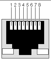
TABLE B-1 provides the eight pin assignments for the Ethernet port connector.
TABLE B-1 Ethernet Port Connector Pin Assignments
|
Pin
|
Signal Name
|
Pin
|
Signal Name
|
|
1
|
DA+
|
5
|
DC-
|
|
2
|
DA-
|
6
|
DB-
|
|
3
|
DB+
|
7
|
DD+
|
|
4
|
DC+
|
8
|
DD-
|
B.3.1.2 USB Ports
FIGURE B-2 shows the connector pin assignments for both of the front panel USB ports.
FIGURE B-2 Front Panel USB Connector

TABLE B-3 lists the USB port connector pin assignments.
TABLE B-2 USB Port Pin Assignments
|
Pin
|
Signal Name
|
Description
|
|
1
|
VCC
|
+5 VDA (500ma)
|
|
2
|
D-
|
Data-
|
|
3
|
D+
|
Data+
|
|
4
|
GND
|
Ground
|
B.3.1.3 Serial Port
FIGURE B-3 shows the connector pin assignments for the front panel serial port.
FIGURE B-3 Front Panel Serial RJ-45 Connector

TABLE B-3 lists the serial port connector pin assignments.
TABLE B-3 Serial Port Mini DIN 8-pin Connector Pinouts
|
Pin
|
Signal Name
|
Pin
|
Signal Name
|
|
1
|
RTS
|
5
|
GND
|
|
2
|
DTR
|
6
|
RXD
|
|
3
|
TXD
|
7
|
DSR
|
|
4
|
GND
|
8
|
CTS
|
B.3.2 AMC Connector
One 170-pin connector provides the AMC connection. The connector and pinouts are defined by the industry-standard specification PICMG Advanced Mezzanine Cards AMC.0 Specification R1.0 ECR-002 D0.9, June 29, 2006.
The AMC slot is available at the front panel. The AMC can be accessed from the front panel, depending on the features of the AMC, or through an optional advanced rear transition module (ARTM).
B.3.3 Power Connector (Zone 1)
The Sun Netra CP3250 blade server uses a 34-pin Positronic connector as the Zone 1 power distribution connector. It provides the support for the following signals:
- Two -48 VDC power feeds (four signals each; eight signals total)
- Two IPMB ports (two signals each; four signals total)
- Geographic address (eight signals)
The analog test and ring voltage pins are left unconnected. FIGURE B-4 shows the pin assignments.
FIGURE B-4 Power Distribution Connector (Zone 1) P10
TABLE B-4 lists the power distribution connector pin assignments.
TABLE B-4 Power Distribution Connector Pin Assignments
|
Pin Number
|
Name
|
Description
|
|
1
|
Reserved
|
Reserved
|
|
2
|
Reserved
|
Reserved
|
|
3
|
Reserved
|
Reserved
|
|
4
|
Reserved
|
Reserved
|
|
5
|
HA0
|
HA0 Hardware Address Bit 0
|
|
6
|
HA1
|
HA1 Hardware Address Bit 1
|
|
7
|
HA2
|
HA2 Hardware Address Bit 2
|
|
8
|
HA3
|
HA3 Hardware Address Bit 3
|
|
9
|
HA4
|
HA4 Hardware Address Bit 4
|
|
10
|
HA5
|
HA5 Hardware Address Bit 5
|
|
11
|
HA6
|
HA6 Hardware Address Bit 6
|
|
12
|
HA7/P
|
HA7/P Hardware Address Bit 7 (Odd Parity Bit)
|
|
13
|
SCL_A
|
IPMB Clock, Port A
|
|
14
|
SDA_A
|
IPMB Data, Port A
|
|
15
|
SCL_B
|
IPMB Clock, Port B
|
|
16
|
SDA_B
|
IPMB Data, Port B
|
|
17
|
MT1_TIP
|
Metallic Test #1 Tip
|
|
18
|
MT1_TIP
|
Metallic Test #2 Tip
|
|
19
|
-RING_A
|
Ringing Generator A Negative Ringing
|
|
20
|
-RING_B
|
Ringing Generator B Negative Ringing
|
|
21
|
MT1_RING
|
Metallic Test #1 Ringing
|
|
22
|
MT2_RING
|
Metallic Test #2 Ringing
|
|
23
|
-RING_A
|
Ringing Generator AReturn
|
|
24
|
-RING_B
|
Ringing Generator B Return
|
|
25
|
SHELF_GND
|
Shelf Ground
|
|
26
|
LOGIC_GND
|
Logic Ground
|
|
27
|
ENABLE_B
|
Enable B
|
|
28
|
VRTN_A
|
Voltage Return A
|
|
29
|
VRTN_B
|
Voltage Return B
|
|
30
|
EARLY_A
|
-48V Early A
|
|
31
|
EARLY_B
|
-48V Early B
|
|
32
|
ENABLE_A
|
Enable A
|
|
33
|
-48V_A
|
-48V A
|
|
34
|
-48V_B
|
-48V B
|
B.3.4 Data Transport Connector (Zone 2)
The data transport connector consists of two 120-pin HM-Zd connectors, labeled P20 and P23, with 40 differential pairs each. These are called the Zone 2 connectors.
The Zone 2 connectors provides the following signals:
- Two 10/100/1000BASE-T/TX Ethernet base fabric channels (four differential signal pairs each; 16 signals total)
- Two 10-Gbit SERDES ports on the extended fabric (eight differential signal pairs each; 32 signals total)
The connector vendor part number is Tyco: 1469001-1.
FIGURE B-5 Zone 2 Connector

TABLE B-5 Zone 2 Connector Pin Assignments
|
Row
No.
|
Interface
Designation
|
J23/P23 Connector Pairs
|
|
ab
|
cd
|
ef
|
gh
|
|
1
|
Fabric Channel 2
|
Tx2[2]+
|
Tx2[2]-
|
Rx2[2]+
|
Rx2[2]-
|
Tx3[2]+
|
Tx3[2]-
|
Rx3[2]+
|
Rx3[2]-
|
|
2
|
Tx0[2]+
|
Tx0[2]-
|
Rx0[2]+
|
Rx0[2]-
|
Tx1[2]+
|
Tx1[2]-
|
Rx1[2]+
|
Rx1[2]-
|
|
3
|
Fabric Channel 1
|
Tx2[1]+
|
Tx2[1]-
|
Rx2[1]+
|
Rx2[1]-
|
Tx3[1]+
|
Tx3[1]-
|
Rx3[1]+
|
Rx3[1]-
|
|
4
|
Tx0[1]+
|
Tx0[1]-
|
Rx0[1]+
|
Rx0[1]-
|
Tx1[1]+
|
Tx1[1]-
|
Rx1[1]+
|
Rx1[1]-
|
|
5
|
Base Channel 1
|
BI_DA1+
(Tx1+)
|
BI_DA1-(Tx1-)
|
BI_DB1+(Rx1+)
|
BI_DB1-(Rx1-)
|
BI_DC1+
|
BI_DC1-
|
BI_DD1+
|
BI_DD1-
|
|
6
|
Base Channel 2
|
BI_DA2+(Tx2+)
|
BI_DA2-(Tx2-)
|
BI_DB2+(Rx2+)
|
BI_DB2-(Rx2-)
|
BI_DC2+
|
BI_DC2-
|
BI_DD2+
|
BI_DD2-
|
|
7
|
n/a
|
unused
|
unused
|
unused
|
unused
|
unused
|
unused
|
unused
|
unused
|
|
8
|
n/a
|
unused
|
unused
|
unused
|
unused
|
unused
|
unused
|
unused
|
unused
|
|
9
|
n/a
|
unused
|
unused
|
unused
|
unused
|
unused
|
unused
|
unused
|
unused
|
|
10
|
n/a
|
unused
|
unused
|
unused
|
unused
|
unused
|
unused
|
unused
|
unused
|
B.3.5 Advanced Rear Transition Module (ARTM) Connector (Zone 3)
The Sun Netra CP3250 blade server provides all the I/O connections for rear access through the Zone 3 advanced rear transition module (ARTM) connector. The connector view and the pinout for the Zone 3 connector are shown in FIGURE B-6.
Zone 3 connector pinouts are presented from the point of view of the ATCA blade, meaning that TX means the ATCA blade is the signal source and the ARTM is the signal receiver. Similarly RX means the ATCA blade is the signal receiver and the ARTM is the signal source.
The “reserved” pins indicate connector pins that are currently reserved for compatibility to all ARTMs. Do not connect signals to reserved pins. The “no connect” indicates pins that should not be connected by the Sun Netra CP3250 blade server.
FIGURE B-6 Zone 3 Connector

B.3.5.1 Zone 3 (J30) Connector Pin Assignments
TABLE B-6 shows the J30 connector pin assignments, used for power signals.
TABLE B-6 J30 Pin Connector Assignments
|
|
1-3
|
4-6
|
Pin Length
|
Mating Sequence
|
|
E
|
PS1#
|
NC
|
short
|
last
|
|
D
|
+12V PP
|
+12V PP
|
long
|
first
|
|
C
|
IPMI_SCL_L
|
IPMI_SDA_L
|
medium
|
Second
|
|
B
|
Logic_GND
|
+3.3V_MP
|
long
|
First
|
|
A
|
Logic_GND
|
Shelf_GND
|
long
|
First
|
B.3.5.2 Zone 3 (J31) Connector PIN Assignments
TABLE B-7 shows the J31 connector pin assignments, used for ARTM signals.
TABLE B-7 J31 Connector Pin Assignments
|
Row
|
Interface
|
AB
|
BG
|
CD
|
DG
|
EF
|
FG
|
|
1
|
AMC0 EO
|
RTM_TX13+ (AMC0 EO_Rx1+)
|
RTM_TX13- (AMC0 EO_Rx1-)
|
GND
|
RTM_RX12+ (AMC0 EO_Tx0+)
|
RTM_RX12- (AMC0 EO_Tx0-)
|
GND
|
RTM_TX12+ (AMC0 EO_Rx0+)
|
RTM_TX12- (AMC0 EO_Rx0-)
|
GND
|
|
2
|
AMC0 EO
|
RTM_RX14+ (AMC0 EO_Tx2+)
|
RTM_RX14- (AMC0 EO_Tx2-)
|
GND
|
RTM_TX14+ (AMC0 EO_Rx2+)
|
RTM_TX14- (AMC0 EO_Rx2-)
|
GND
|
RTM_RX13+ (AMC0 EO_Tx1+)
|
RTM_RX13- (AMC0 EO_Tx1-)
|
GND
|
|
3
|
AMC0 EO
|
RTM_TX17+ (AMC0 EO_Rx4+)
|
RTM_TX17- (AMC0 EO_Rx4-)
|
GND
|
RTM_RX15+ (AMC0 EO_Tx3+)
|
RTM_RX15- (AMC0 EO_Tx3-)
|
GND
|
RTM_TX15+ (AMC0 EO_Rx3+)
|
RTM_TX15- (AMC0 EO_Rx3-)
|
GND
|
|
4
|
AMC0 EO
|
RTM_RX18+ (AMC0 EO_Tx5+)
|
RTM_RX18- (AMC0 EO_Tx5-)
|
GND
|
RTM_TX18+ (AMC0 EO_Rx5+)
|
RTM_TX18- (AMC0 EO_Rx5-)
|
GND
|
RTM_RX17+ (AMC0 EO_Tx4+)
|
RTM_RX17- (AMC0 EO_Tx4-)
|
GND
|
|
5
|
AMC0 EO
|
RTM_TX20+ (AMC0 EO_Rx7+)
|
RTM_TX20- (AMC0 EO_Rx7-)
|
GND
|
RTM_RX19+ (AMC0 EO_Tx6+)
|
RTM_RX19- (AMC0 EO_Tx6-)
|
GND
|
RTM_TX19+ (AMC0 EO_Rx6+)
|
RTM_TX19- (AMC0 EO_Rx6-)
|
GND
|
|
6
|
AMC0 EO
|
Reserved
|
Reserved
|
GND
|
Reserved
|
Reserved
|
GND
|
RTM_RX20+ (AMC0 EO_Tx7+)
|
RTM_RX20- (AMC0 EO_Tx7-)
|
GND
|
|
7
|
Reserved
|
Reserved
|
Reserved
|
GND
|
Reserved
|
Reserved
|
GND
|
Reserved
|
Reserved
|
GND
|
|
8
|
Reserved
|
Reserved
|
Reserved
|
GND
|
Reserved
|
Reserved
|
GND
|
Reserved
|
Reserved
|
GND
|
|
9
|
Reserved
|
Reserved
|
Reserved
|
GND
|
Reserved
|
Reserved
|
GND
|
Reserved
|
Reserved
|
GND
|
|
10
|
Reserved
|
Reserved
|
Reserved
|
GND
|
Reserved
|
Reserved
|
GND
|
Reserved
|
Reserved
|
GND
|
B.3.5.3 Zone 3 (J32) Connector PIN Assignments
TABLE B-8 shows the J32 connector pin assignments, used for ARTM signals.
TABLE B-8 J32 Connector Pin Assignments
|
Row
|
Interface
|
AB
|
BG
|
CD
|
DG
|
EF
|
FG
|
|
1
|
Reserved
|
Reserved
|
Reserved
|
GND
|
Reserved
|
Reserved
|
GND
|
Reserved
|
Reserved
|
GND
|
|
2
|
SAS AMC0
|
SAS TX0+ (AMC0 SAS0_Rx+)
|
SAS TX0- (AMC0 SAS0_Rx-)
|
GND
|
SAS RX0+ (AMC0 SAS0_Tx+)
|
SAS RX0- (AMC0 SAS0_Tx-)
|
GND
|
RTS (Serial 0)
|
DTR (Serial 0)
|
GND
|
|
3
|
Reserved
|
Reserved
|
Reserved
|
GND
|
Reserved
|
Reserved
|
GND
|
TXD (Serial 0)
|
RXD (Serial 0)
|
GND
|
|
4
|
SAS AMC0
|
SAS TX2+ (AMC0 SAS1_Rx+)
|
SAS TX2- (AMC0 SAS1_Rx+)
|
GND
|
SAS RX2+ (AMC0 SAS1_Rx+)
|
SAS RX2- (AMC0 SAS1_Rx+)
|
GND
|
DSR (Serial 0)
|
CTS (Serial 0)
|
GND
|
|
5
|
Reserved
|
Reserved
|
Reserved
|
GND
|
Reserved
|
Reserved
|
GND
|
No Connect
|
No Connect
|
GND
|
|
6
|
RTM LAN0 (Mgmt)
|
LAN0_A+
|
LAN0_A-
|
GND
|
LAN0_CTV
|
LAN0_CTV
|
GND
|
LAN0_B+
|
LAN0_B-
|
GND
|
|
7
|
RTM LAN0 (Mgmt)
|
LAN0_C+
|
LAN0_C-
|
GND
|
ACT_LED#
|
LINK_LED#
|
GND
|
LAN0_D+
|
LAN0_D-
|
GND
|
|
8
|
RTM LAN1 (SerDes)
|
SLAN_TX1+
|
SLAN_TX1-
|
GND
|
SLAN_RX1+
|
SLAN_RX1-
|
GND
|
No Connect
|
No Connect
|
GND
|
|
9
|
RTM LAN2/LAN4 (SerDes)
|
SLAN_TX2+
|
SLAN_TX2-
|
GND
|
SLAN_RX2+
|
SLAN_RX2-
|
GND
|
SLAN_TX4+
|
SLAN_TX4-
|
GND
|
|
10
|
RTM LAN3/LAN4 (SerDes)
|
SLAN_TX3+
|
SLAN_TX3-
|
GND
|
SLAN_RX3+
|
SLAN_RX3-
|
GND
|
SLAN_RX4+
|
SLAN_RX4-
|
GND
|
B.3.5.4 Zone 3 (J33) Connector PIN Assignments
TABLE B-9 shows the J33 connector pin assignments, which are used ARTM signals.
TABLE B-9 J33 Connector Pin Assignments
|
Row
|
Interface
|
AB
|
BG
|
CD
|
DG
|
EF
|
FG
|
|
1
|
PCIe x8 Lane
|
PETx0+
|
PETx0-
|
GND
|
PERx0+
|
PERx0-
|
GND
|
FCLKA+
|
FCLKA-
|
GND
|
|
2
|
PCIe x8 Lane
|
PETx1+
|
PETx1-
|
GND
|
PERx1+
|
PERx1-
|
GND
|
TCLKA+
|
TCLKA-
|
GND
|
|
3
|
PCIe x8 Lane
|
PETx2+
|
PETx2-
|
GND
|
PERx2+
|
PERx2-
|
GND
|
TCLKB+
|
TCLKB-
|
GND
|
|
4
|
PCIe x8 Lane
|
PETx3+
|
PETx3-
|
GND
|
PERx3+
|
PERx3-
|
GND
|
TCLKC+
|
TCLKC-
|
GND
|
|
5
|
PCIe x8 Lane
|
PETx4+
|
PETx4-
|
GND
|
PERx4+
|
PERx4-
|
GND
|
TCLKD+
|
TCLKD-
|
GND
|
|
6
|
PCIe x8 Lane
|
PETx5+
|
PETx5-
|
GND
|
PERx5+
|
PERx5-
|
GND
|
TCK
|
TMS
|
GND
|
|
7
|
PCIe x8 Lane
|
PETx6+
|
PETx6-
|
GND
|
PERx6+
|
PERx6-
|
GND
|
TRST#
|
TDO
|
GND
|
|
8
|
PCIe x8 Lane
|
PETx7+
|
PETx7-
|
GND
|
PERx7+
|
PERx7-
|
GND
|
TDI
|
PCI_RST#
|
GND
|
|
9
|
Reserved
|
No Connect
|
No Connect
|
GND
|
No Connect
|
No Connect
|
GND
|
ARTM#
|
PCI_CFG
|
GND
|
|
10
|
Reserved
|
No Connect
|
No Connect
|
GND
|
No Connect
|
No Connect
|
GND
|
PS0#
|
Enabled#
|
GND
|
B.3.5.5 Zone 3 Signal Descriptions
TABLE B-10 provides descriptions of the signals listed in the Zone 3 pin assignment tables (TABLE B-6 through TABLE B-9).
TABLE B-10 Zone 3 Signal Descriptions
|
Signal Name
|
Description
|
|
IPMI_SCL_L
|
IPMI bus clock signal, as defined in AMC.0 specification. RTM shall have a pull-up resistor for this signal as indicated in AMC.0 specification.
|
|
IPMI_SDA_L
|
IPMI bus data signal, as defined in AMC.0 specification. RTM shall have a pull-up resistor for this signal as indicated in AMC.0 specification.
|
|
PS0#, PS1#
|
Active low RTM present signal.PS0# shall be tied to logic GND on the ATCA blade, PS1# shall be pulled up to 3.3V Management Power on the ATCA blade, PS0# and PS1# shall be connected through diode on RTM, exactly as defined in AMC.0 specification. PS1# is last mate on Power connector and PS0# is on the opposite end of the set of connectors. Logic low on PS1# indicates that RTM is present and fully inserted.
|
|
Enable#
|
When low indicates to RTM that it is fully inserted and that MMC can start execution. Logic high shall keep MMC in reset state. This signal shall have a pull-up resistor as indicated in AMC.0 specification.
|
|
Shelf_GND
|
Frame/Chassis Safety Ground.
|
|
Logic_GND
|
(Logic 0vdc). Logic Ground- Common return for Management Power Payload Power, reference potential for single-ended logic signaling, and shielding for differential pair signals in the AMC Connector.
|
|
12VPP
|
12V Payload Power, enabled after successful E-keying, following AMC.0 specification. RTM shall meet requirements posted for payload power in AMC specification.
|
|
3.3V_MP
|
3.3V Management Power. RTM shall meet requirements posted for management power in AMC.0 specification.
|
|
RTM_RX
|
AMC Extended Options receive differential pair signals. Note that this specification takes ATCA Blade perspective, which means that RX signals are driven by RTM and received by ATCA Blade.
|
|
RTM_TX
|
AMC Extended Options transmit differential pair signals. Note that this specification takes ATCA Blade perspective, which means that TX signals are driven by ATCA Blade and received by RTM.
|
|
SAS_TX
|
SATA/SAS transmit differential pair signals.
|
|
SAS_RX
|
SATA/SAS receive differential pair signals.
|
|
Serial 0
|
RS-232 Serial Signals, Transmit, Receive, Clear to Send, Request to Send, Data Terminal Ready, and Data Set Ready.
|
|
LAN0
|
10/100/1000BASE-T signals.
|
|
LAN0_CTV
|
10/100/1000BASE-T transformer Center Tap signal, which could be used to terminate center tap of transformers, if they are placed on RTM. This signal is applicable if Ethernet PHY is located on ATCA blade, while transformers are located on RTM.
|
|
ACT_LED#
|
LAN 0 (Management) activity indicator signal for LED (active low).
|
|
LINK_LED#
|
LAN 0 (Management) LINK indicator signal for LED (active low).
|
|
PCI_CFG
|
PCI Express bus configuration signal. It shall be grounded on RTMs that use a single x8 PCI Express bus and pulled up on the ATCA with 10Kohm resistor to management power. On RTMs that expect two x4 PCI-Express busses this pin will float (not be connected). Two x4 PCI-Express busses are intended for RTM implementations that desire to avoid PCI-Express switch in order to reduce latency.
|
|
ARTM#
|
ARTM# signal shall be grounded on ARTMs that implement MMC controller as defined by AMC.0 specification. This signal shall be pulled up with 10Kohm resistor to management power on the ATCA node blade server.
|
|
SLAN_TX
|
GBEthernet SerDes transmit differential pair signals.
|
|
SLAN_RX
|
GBEthernet SerDes receive differential pair signals.
|
|
PETx
|
PCI-Express transmit differential pair signals.
|
|
PERx
|
PCI-Express receive differential pair signals.
|
|
PCI_RST#
|
PCI-Express reset signal. Logic low shall reset downstream PCI-Express devices on ARTM.
|
|
TCLKA
|
PCI-Telecom clock A 19.44MHz, differential pair into RTM (ATCA CLK2) as defined in AMC.0 specification.
|
|
TCLKB
|
PCI-Telecom clock B 19.44MHz, differential pair out from RTM (ATCA CLK3) as defined in AMC.0 specification.
|
|
TCLKC
|
PCI-Telecom clock C 8kHz, differential pair into RTM (ATCA CLK1) as defined in AMC.0 specification.
|
|
TCLKD
|
PCI-Telecom clock D 8kHz, differential pair out from RTM as defined in AMC.0 specification.
|
|
FCLKA
|
Fabric clock, as defined in AMC.0 specification. Intended to be used for PCI-Express 100 MHz spread spectrum clock.
|
|
TCK, TMS, TRST#, TDO, TDI
|
JTAG signals. Signal direction shall follow AMC.0 specification.
|
| Sun Netra CP3250 Blade Server User’s Guide
|
820-5195-11
|
   
|
Copyright © 2009 Sun Microsystems, Inc. All rights reserved.