| Netra CP3010 Board User's Guide
|
   
|
Specifications for the Netra CP3010 board are provided in the following sections:
A.1 Form Factor
The Netra CP3010 board is a standard 8U form factor, a single slot wide, and complies with the board mechanical dimensions required by the PICMG 3.0 R1.0 Specification:
- 322.25 mm x 280 mm (length by width)
- 1.2-inch-wide front panel
A.2 Thermal Management
A heat sink was designed for each UltraSPARC IIIi and JBus-PCI bridge pair. The heat sink is mechanically mounted to the Netra CP3010 board. The heat sink and DIMMs are positioned with respect to the overall board airflow (bottom to top).
A.3 Layout
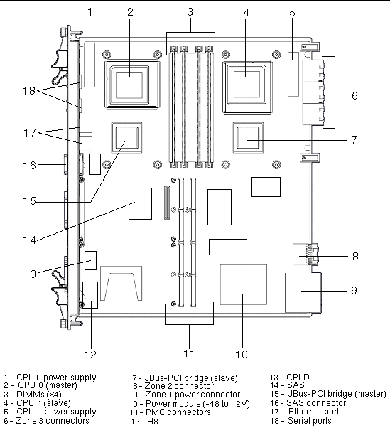
The Netra CP3010 board layout is shown in FIGURE A-1.
FIGURE A-1 Netra CP3010 Board Layout

A.4 Front Panel
The single-slot-wide, 8U front panel was designed to meet PICMG 3.0 R 1.0 and other specifications.
A.4.1 Visual Indicators
The Netra CP3010 board has the following indicators on the front panel:
- Green LED - Board's healthy status or user programmable (ACTIVE).
- Yellow LED - Board's fault condition (FAULT).
- Blue LED - Indicates safe removal (hot-swap activity).
The front panel's Ethernet ports do not have LED indicators.
A.5 Switches and Jumpers
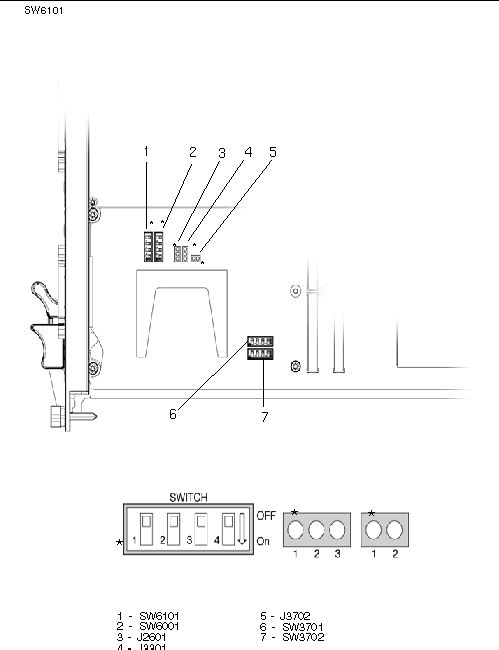
There are four switches, two three-pronged jumpers, and one two-prong jumper on the Netra CP3010 board assembly. They are located on the primary side of the printed circuit board (PCB) between the front panel and the PMC #1 connectors. See FIGURE A-2 for details.
Each switch has four positions: 1 to 4. Each position can be OFF or ON. Each jumper can be shorted (or jumped) to an adjacent pin. The star (*) on the PCB by the jumpers indicates pin 1 (see FIGURE A-2). TABLE A-1 shows the switches and TABLE A-2 jumpers for operation.
FIGURE A-2 Switches and Jumpers

TABLE A-1 Switch Setting
|
Switch
|
Position 1
|
Position 2
|
Position 3
|
Position 4
|
|
OFF
|
ON
|
OFF
|
ON
|
OFF
|
ON
|
OFF
|
ON
|
|
SW3701
|
Config bit
no effect
[default]
|
Config bit
no effect
|
Config bit
no effect
[default]
|
Config bit
no effect
|
Config bit
no effect
[default]
|
Config bit
no effect
|
Config bit
no effect
[default]
|
Config bit
no effect
|
|
SW3702
|
Config bit
no effect
[default]
|
Config bit
no effect
|
Config bit
no effect
[default]
|
Config bit
no effect
|
Not connected
|
Not connected
|
|
SW6001
|
MD2* mode Bit2 =1
|
MD2* mode Bit2 =0
[default]
|
MD1 mode Bit1 =1
[default]
|
MD1 mode Bit1 =0
|
H8 Non-Maskable Interrupt NMI=1 (enabled)
[default]
|
H8 Non-Maskable Interrupt NMI=0 (disabled)
|
H8 Flash Write Enable FWE=1 (enabled)
[default]
|
H8 Flash Write Enable FWE=0 (disabled)
|
|
SW6101
|
Bootpage bit 0 =1
|
Bootpage bit 0 =0
[default]
|
Bootpage bit 1 =1
|
Bootpage bit 1 =0
[default]
|
Serial hardware flow control OFF
|
Serial hardware flow control ON
[default]
|
H8 controls power on (stand-alone)
|
Hardware controls power on (in chassis)
[default]
|
|
Note - The MD2*, MD1, NMI, and FWE defaults set the H8 to mode 2, User Programming mode.
|
TABLE A-2 Jumper Settings
|
Jumper
|
Open
|
Short Pin 1 to Pin 2
|
Short Pin 2 to Pin 3
|
|
J2601
|
Normal operation
[default]
|
Force power-on reset
|
Force XIR reset
|
|
J3301
|
Do not use
|
Normal operation
[default]
|
Clear Real-Time_Clock
|
|
J3702
|
Write protect SUN FRU ID [default]
|
Enable write of SUN FRU ID
|
N/A
|
A.6 Connectors and Pinout
FIGURE A-1 shows all the basic I/O connectors to the front and the rear of the Netra CP3010 board. Also shown is the placement of the PMC connectors.
A.6.1 Front Panel Connectors
The front panel has the following connectors:
- Two 10/100BASE-T Ethernet ports (RJ-45)
- Two serial ports (SubDB-9)
- One 4X SAS port (supports only two SAS channels)
A.6.1.1 Ethernet Ports
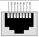
The Ethernet connectors are RJ-45 connectors. The controller autonegotiates to either 10BASE-T or 100BASE-T. The Ethernet connector pin numbering is shown in FIGURE A-3.
FIGURE A-3 Ethernet RJ-45 Connector

TABLE A-3 shows the Ethernet connector pin assignments.
TABLE A-3 Ethernet Port Connector Pin Assignments
|
Pin
|
Signal Name
|
Pin
|
Signal Name
|
|
1
|
TXD+
|
5
|
Not used
|
|
2
|
TXD-
|
6
|
RXD-
|
|
3
|
RXD+
|
7
|
Not used
|
|
4
|
Not Used
|
8
|
Not used
|
A.6.1.2 Serial Ports
FIGURE A-4 contains the connector pin assignments for the front panel serial port.
FIGURE A-4 Front Panel Serial Port Diagram

TABLE A-4 shows the serial port connector pin assignments.
TABLE A-4 Serial Port Mini Din 8-pin Connector Pinouts
|
Pin
|
Signal Name
|
Pin
|
Signal Name
|
|
1
|
RTS
|
5
|
DCD
|
|
2
|
DTR
|
6
|
RXD
|
|
3
|
TXD
|
7
|
DSR
|
|
4
|
GND
|
8
|
CTS
|
A.6.1.3 SAS Port
The Netra CP3010 board provides a Serial Attached SCSI (SAS) port using a standard 4x SAS port connector. Only two SAS channels are routed to the 4x port connector. The SAS access is through both the front panel and the rear; the rear access requires the RTM.
A.6.2 PMC Connectors
There are four 64-pin connectors that make up the PMC card connection. These connectors and pinouts are defined by the following industry-standard specifications:
- Draft Standard Physical and Environmental Layers for PCI Mezzanine Cards: PMC IEEE (MMSC) P1386.1/Draft 2.3, October 9, 2000
- Draft Standard for a Common Mezzanine Card Family: CMC IEEE (MMSC) P1386/Draft 2.3, October 9, 2000
The PMC slots are available on the front panel. The PMC I/O transactions are passed to the RTM and are available using PIM cards and cables.
A.6.3 Backplane Power Connector (Zone 1)
The Netra CP3010 board uses a 34-pin Positronic connector as the Zone 1 power connector. It provides support for the following signals:
- Two -48 volt DC power feeds (four signals each; eight signals total)
- Two IPMB ports (two signals each, four signals total)
- Geographic address (eight signals)
The analog test and ring voltage pins are left unconnected.
FIGURE A-5 shows the pin assignments.
FIGURE A-5 Power Distribution Connector (Zone 1) P10

TABLE A-5 lists the power connector pin assignments.
TABLE A-5 Power Distribution Connector Pin Assignments
|
Pin Number
|
Name
|
Description
|
|
1
|
Reserved
|
Reserved
|
|
2
|
Reserved
|
Reserved
|
|
3
|
Reserved
|
Reserved
|
|
4
|
Reserved
|
Reserved
|
|
5
|
HA0
|
HA0 Hardware Address Bit 0
|
|
6
|
HA1
|
HA1 Hardware Address Bit 1
|
|
7
|
HA2
|
HA2 Hardware Address Bit 2
|
|
8
|
HA3
|
HA3 Hardware Address Bit 3
|
|
9
|
HA4
|
HA4 Hardware Address Bit 4
|
|
10
|
HA5
|
HA5 Hardware Address Bit 5
|
|
11
|
HA6
|
HA6 Hardware Address Bit 6
|
|
12
|
HA7/P
|
HA7/P Hardware Address Bit 7(Odd Parity Bit)
|
|
13
|
SCL_A
|
IPMB Clock, Port A
|
|
14
|
SDA_A
|
IPMB Data, Port A
|
|
15
|
SCL_B
|
IPMB Clock, Port B
|
|
16
|
SDA_B
|
IPMB Data, Port B
|
|
17
|
Unused
|
|
|
18
|
Unused
|
|
|
19
|
Unused
|
|
|
20
|
Unused
|
|
|
21
|
Unused
|
|
|
22
|
Unused
|
|
|
23
|
Unused
|
|
|
24
|
Unused
|
|
|
25
|
SHELF_GND
|
Shelf Ground
|
|
26
|
LOGIC_GND
|
Logic Ground
|
|
27
|
ENABLE_B
|
Enable B
|
|
28
|
VRTN_A
|
Voltage Return A
|
|
29
|
VRTN_B
|
Voltage Return B
|
|
30
|
EARLY_A
|
-48V Early A
|
|
31
|
EARLY_B
|
-48V Early B
|
|
32
|
ENABLE_A
|
Enable A
|
|
33
|
-48V_A
|
-48V A
|
|
34
|
-48V_B
|
-48V B
|
A.6.4 Data Transport Connector (Zone 2)
The data transport connector consists of one 120-pin HM-Zd connector, labeled P23, with 40 differential pairs. This is called the Zone 2 connector.
The Zone 2 connector provides the following signals:
- Two 10/100BASE-T/TX Ethernet Base Fabric channels (four differential signal pairs each, 16 signals total)
- Two 2-Gb SERDES ports on the Extended Fabric interface (2 differential signal pairs each, 8 signals total)
The connector vendor part number is Tyco: 1469001-1. FIGURE A-6 shows the Zone 2 connector.
FIGURE A-6 Zone 2 Connector

A.6.5 RTM Connector (Zone 3)
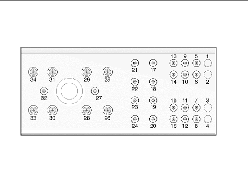
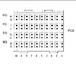
The Netra CP3010 board provides all the I/O connections for rear access through the Zone 3 RTM connector. The connector view and the pinout for the Zone 3 connectors is shown in FIGURE A-7.
FIGURE A-7 Zone 3 Connector

TABLE A-6 gives the Zone 3 J6402 connector pin assignments.
TABLE A-6 J6402 Connector Pin Assignments
|
Row
|
A
|
B
|
BG
|
C
|
D
|
DG
|
E
|
F
|
FG
|
|
1
|
PMC1_IO1
|
PMC1_IO2
|
|
PMC1_IO3
|
PMC1_IO4
|
|
PMC1_IO5
|
PMC1_IO6
|
GND
|
|
2
|
PMC1_IO7
|
PMC1_IO8
|
|
PMC1_IO9
|
PMC1_IO10
|
|
PMC1_IO11
|
PMC1_IO12
|
|
|
3
|
PMC1_IO13
|
PMC1_IO14
|
|
PMC1_IO15
|
PMC1_IO16
|
|
PMC1_IO17
|
PMC1_IO18
|
|
|
4
|
PMC1_IO19
|
PMC1_IO20
|
|
PMC1_IO21
|
PMC1_IO22
|
|
PMC1_IO23
|
PMC1_IO24
|
|
|
5
|
PMC1_IO25
|
PMC1_IO26
|
|
PMC1_IO27
|
PMC1_IO28
|
|
PMC1_IO29
|
PMC1_IO30
|
|
|
6
|
PMC1_IO31
|
PMC1_IO32
|
|
PMC1_IO33
|
PMC1_IO34
|
|
PMC1_IO35
|
PMC1_IO36
|
GND
|
|
7
|
PMC1_IO37
|
PMC1_IO38
|
|
PMC1_IO39
|
PMC1_IO40
|
|
PMC1_IO41
|
PMC1_IO42
|
|
|
8
|
PMC1_IO43
|
PMC1_IO44
|
|
PMC1_IO45
|
PMC1_IO46
|
|
PMC1_IO47
|
PMC1_IO48
|
|
|
9
|
PMC1_IO49
|
PMC1_IO50
|
|
PMC1_IO51
|
PMC1_IO52
|
|
PMC1_IO53
|
PMC1_IO54
|
|
|
10
|
PMC1_IO55
|
PMC1_IO56
|
|
PMC1_IO57
|
PMC1_IO58
|
|
PMC1_IO59
|
PMC1_IO60
|
|
TABLE A-7 gives the Zone 3 J6401 connector pin assignments.
TABLE A-7 J6401 Connector Pin Assignments
|
Row
|
A
|
B
|
BG
|
C
|
D
|
DG
|
E
|
F
|
FG
|
|
1
|
PMC0_IO1
|
PMC0_IO2
|
|
PMC0_IO3
|
PMC0_IO4
|
|
PMC0_IO5
|
PMC0_IO6
|
GND
|
|
2
|
PMC0_IO7
|
PMC0_IO8
|
|
PMC0_IO9
|
PMC0_IO10
|
|
PMC0_IO11
|
PMC0_IO12
|
|
|
3
|
PMC0_IO24
|
PMC0_IO23
|
|
PMC0_IO22
|
PMC0_IO21
|
|
PMC0_IO20
|
PMC0_IO19
|
|
|
4
|
PMC0_IO18
|
PMC0_IO17
|
|
PMC0_IO16
|
PMC0_IO15
|
GND
|
PMC0_IO14
|
PMC0_IO13
|
|
|
5
|
PMC0_IO36
|
PMC0_IO35
|
GND
|
PMC0_IO34
|
PMC0_IO33
|
|
PMC0_IO32
|
PMC0_IO31
|
|
|
6
|
PMC0_IO30
|
PMC0_IO29
|
|
PMC0_IO28
|
PMC0_IO27
|
|
PMC0_IO26
|
PMC0_IO25
|
|
|
7
|
PMC0_IO48
|
PMC0_IO47
|
|
PMC0_IO46
|
PMC0_IO45
|
GND
|
PMC0_IO44
|
PMC0_IO43
|
|
|
8
|
PMC0_IO42
|
PMC0_IO41
|
|
PMC0_IO40
|
PMC0_IO39
|
|
PMC0_IO38
|
PMC0_IO37
|
|
|
9
|
PMC0_IO49
|
PMC0_IO50
|
|
PMC0_IO51
|
PMC0_IO52
|
|
PMC0_IO53
|
PMC0_IO54
|
|
|
10
|
PMC0_IO55
|
PMC0_IO56
|
|
PMC0_IO57
|
PMC0_IO58
|
|
PMC0_IO59
|
PMC0_IO60
|
|
TABLE A-8 gives the Zone 3 J6501 connector pin assignments.
TABLE A-8 J6501 Connector Pin Assignments
|
Row
|
A
|
B
|
BG
|
C
|
D
|
DG
|
E
|
F
|
FG
|
|
1
|
PMC0_IO61
|
PMC1_IO2
|
|
PMC0_IO63
|
PMC0_IO64
|
|
|
-12V
|
GND
|
|
2
|
PMC1_IO61
|
PMC1_IO8
|
5V
|
PMC1_IO63
|
PMC1_IO64
|
5V
|
+12V
|
+12V
|
|
|
3
|
RTM_SER1_CTS
|
PMC1_IO14
|
3.3V
|
RTM_SER1_DCD
|
RTM_SER1_DSR
|
3.3V
|
RTM_SER1_RXD
|
RTM_SER1_TXD
|
|
|
4
|
RTM_SER1_RTS
|
PMC1_IO20
|
3.3V
|
RTM_SER2_CTS
|
RTM_SER2_DTR
|
3.3V
|
RTM_SER2_DCD
|
RTM_SER2_DSR
|
|
|
5
|
RTM_SER2_RXD
|
PMC1_IO26
|
5V
|
RTM_SER2_RTS
|
|
5V
|
|
|
|
|
6
|
RTM_HDD2_RX_P
|
PMC1_IO32
|
GND
|
|
|
GND
|
RTM_HDD2_TX_N
|
RTM_HDD2_TX_P
|
|
|
7
|
RTM_PRSNT_N
|
PMC1_IO38
|
GND
|
SYS_I2C_SDA
|
SYS_I2C_SCL
|
GND
|
3V_STBY
|
3V_STBY
|
|
|
8
|
RTM_HDD3_RX_P
|
PMC1_IO44
|
GND
|
|
|
GND
|
RTM_HDD3_TX_N
|
RTM_HDD3_TX_P
|
|
|
9
|
RTM_TXD_1P
|
PMC1_IO50
|
GND
|
2.5V
|
2.5V
|
GND
|
RTM_RXD_1P
|
RTM_RXD_1N
|
|
|
10
|
RTM_TXD_0P
|
PMC1_IO56
|
GND
|
2.5V
|
2.5V
|
GND
|
RTM_RXD_0P
|
RTM_RXD_0N
|
|
| Netra CP3010 Board User's Guide
|
819-1183-10
|
   
|
Copyright © 2006, Sun Microsystems, Inc. All Rights Reserved.
