Specifications for the Netra CP3260 blade server are provided in the following sections:
A.1 Form Factor
The Netra CP3260 blade server is a standard 8U form factor, a single-slot-wide. It complies with the blade server mechanical dimensions required by the PICMG 3.0 R1.0 Specification:
- 322.25 mm x 280 mm (length x width)
- 1.2-inch-wide front panel
A.2 Layout
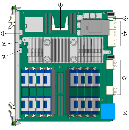
The Netra CP3260 blade server layout is shown in FIGURE A-1.
FIGURE A-1 Netra CP3260 Blade Server Layout

.
Figure Legend
|
1
|
Ethernet port connector (RJ-45)
|
5
|
Zone 1 power connector
|
|
2
|
Dual USB port connector (USB 2.0)
|
6
|
Zone 2 I/O connectors
|
|
3
|
Serial port connector
|
7
|
Zone 3 RTM I/O connectors
|
|
4
|
Compact flash connector
|
8
|
Zone 3 RTM power connector
|
A.3 Front Panel
The single-slot-wide, 8U front panel was designed to meet PICMG 3.0 R 1.0 and other specifications.
A.3.1 Visual Indicators
The Netra CP3260 blade server has the following indicators on the front panel:
- Green LED - Board’s healthy status or user programmable (ACTIVE).
- Amber LED - Board’s fault condition (FAULT).
- Blue LED - Indicates safe removal (hot-swap activity).
The front panel’s Ethernet ports do not have LED indicators.
A.3.2 Ports
The Netra CP3260 blade server has the following ports on the front panel:
- One 10/100/1000BASE-T Ethernet port (RJ-45)
- Dual USB ports (USB 2.0)
- One serial port (RJ-45)
A.4 Connectors and Pinout
FIGURE A-1 shows all the basic I/O connectors to the front and the rear of the Netra CP3260 blade server.
A.4.1 Front Panel Connectors
The front panel has the following connectors:
- One 10/100/1000BASE-T Ethernet port (RJ-45)
- One serial port (RJ-45)
- Dual USB ports (USB 2.0)
A.4.1.1 Ethernet Port
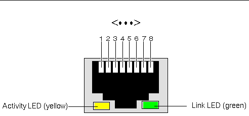
The Ethernet connector is a RJ-45 connector. The controller autonegotiates to either 10BASE-T, 100BASE-T, or 1000BASE-T. The Ethernet connector pin numbering is shown in FIGURE A-2.
FIGURE A-2 Ethernet RJ-45 Connector

TABLE A-1 shows the Ethernet connector pin assignments.
TABLE A-1 Ethernet Port Connector Pin Assignments
|
Pin
|
Signal Name
|
Function
|
Pin
|
Signal Name
|
Function
|
|
1
|
BI_DA+
|
Bi-directional pair +A
|
5
|
BI_DC-
|
Bi-directional pair +C
|
|
2
|
BI_DA-
|
Bi-directional pair -A
|
6
|
BI_DB-
|
Bi-directional pair -C
|
|
3
|
BI_DB+
|
Bi-directional pair +B
|
7
|
BI_DD+
|
Bi-directional pair +D
|
|
4
|
BI_DC+
|
Bi-directional pair -B
|
8
|
BI_DD-
|
Bi-directional pair -D
|
A.4.1.2 Dual USB Port
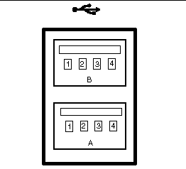
The dual-port Universal Serial Bus (USB) connector pin numbering is shown in FIGURE A-3.
FIGURE A-3 Dual USB Connector

For USB connector signals, see TABLE A-2.
TABLE A-2 USB Connector Pin Assignments
|
Pin
|
Signal Description
|
Pin
|
Signal Description
|
|
A1
|
+5 V (fused)
|
B1
|
+5 V (fused)
|
|
A2
|
USB2-
|
B2
|
USB3-
|
|
A3
|
USB2+
|
B3
|
USB3+
|
|
A4
|
Ground
|
B4
|
Ground
|
A.4.1.3 Serial Port
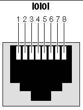
FIGURE A-4 contains the connector pin assignments for the front panel serial port.
FIGURE A-4 Front Panel Serial Port Diagram

TABLE A-3 shows the serial port connector pin assignments.
TABLE A-3 Serial Port RJ-45 Connector Pinouts
|
Pin
|
Signal
Name
|
Function
|
Pin
|
Signal
Name
|
Function
|
|
1
|
RTS
|
Request To Send
|
5
|
GND
|
Ground
|
|
2
|
DTR
|
Data Terminal Ready
|
6
|
RXD
|
Receive Data
|
|
3
|
TXD
|
Transmit Data
|
7
|
DSR
|
Data Set Ready
|
|
4
|
GND
|
Ground
|
8
|
CTS
|
Clear To Send
|
A.4.2 Compact Flash Connector
The Compact Flash connector is a type I/II connector.
A.4.3 Midplane Power Connector (Zone 1)
The Netra CP3260 blade server uses a Zone 1 power connector. It provides support for the following signals:
- Two -48 volt DC power feeds (four signals each; eight signals total)
- Two IPMB ports (two signals each, four signals total)
- Geographic address (eight signals)
The analog test and ring voltage pins are left unconnected.
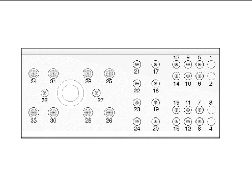
FIGURE A-5 shows the pin assignments.
FIGURE A-5 Power Distribution Connector (Zone 1) P10

TABLE A-4 lists the power connector pin assignments.
TABLE A-4 Power Distribution Connector Pin Assignments
|
Pin Number
|
Name
|
Description
|
|
1
|
Reserved
|
Reserved
|
|
2
|
Reserved
|
Reserved
|
|
3
|
Reserved
|
Reserved
|
|
4
|
Reserved
|
Reserved
|
|
5
|
HA0
|
HA0 Hardware Address Bit 0
|
|
6
|
HA1
|
HA1 Hardware Address Bit 1
|
|
7
|
HA2
|
HA2 Hardware Address Bit 2
|
|
8
|
HA3
|
HA3 Hardware Address Bit 3
|
|
9
|
HA4
|
HA4 Hardware Address Bit 4
|
|
10
|
HA5
|
HA5 Hardware Address Bit 5
|
|
11
|
HA6
|
HA6 Hardware Address Bit 6
|
|
12
|
HA7/P
|
HA7/P Hardware Address Bit 7(Odd Parity Bit)
|
|
13
|
SCL_A
|
IPMB Clock, Port A
|
|
14
|
SDA_A
|
IPMB Data, Port A
|
|
15
|
SCL_B
|
IPMB Clock, Port B
|
|
16
|
SDA_B
|
IPMB Data, Port B
|
|
17
|
Unused
|
|
|
18
|
Unused
|
|
|
19
|
Unused
|
|
|
20
|
Unused
|
|
|
21
|
Unused
|
|
|
22
|
Unused
|
|
|
23
|
Unused
|
|
|
24
|
Unused
|
|
|
25
|
SHELF_GND
|
Shelf Ground
|
|
26
|
LOGIC_GND
|
Logic Ground
|
|
27
|
ENABLE_B
|
Enable B
|
|
28
|
VRTN_A
|
Voltage Return A
|
|
29
|
VRTN_B
|
Voltage Return B
|
|
30
|
EARLY_A
|
-48V Early A
|
|
31
|
EARLY_B
|
-48V Early B
|
|
32
|
ENABLE_A
|
Enable A
|
|
33
|
-48V_A
|
-48V A
|
|
34
|
-48V_B
|
-48V B
|
A.4.4 Data Transport Connector (Zone 2)
The data transport connector consists of one 120-pin HM-Zd connector, labeled P23, with 40 differential pairs. This is called the Zone 2 connector.
The Zone 2 connector provides the following signals:
- Two 1000BASE-T Ethernet Base interface channels
- Two 1-Gb SERDES on the Fabric (extended) interface
- 10-Gb XAUI on the Fabric (extended) interface
- Synchronization Clock interface supporting CLK1A/B and CLK2A/2B
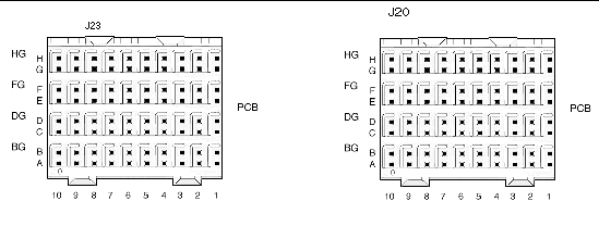
FIGURE A-6 shows the Zone 2 connectors.
FIGURE A-6 Zone 2 Connectors

TABLE A-5 gives the Zone 2 J23 connector pin assignments.
TABLE A-5 Zone 2 J23 Connector Pin Assignments
|
Row
|
A
|
B
|
C
|
D
|
E
|
F
|
G
|
H
|
|
1
|
P23_F2_TX2+
|
P23_F2_TX2-
|
P23_F2_RX2+
|
P23_F2_RX2-
|
P23_F2_TX3+
|
P23_F2_TX3-
|
P23_F2_RX3+
|
P23_F2_RX3-
|
|
2
|
P23_F2_TX0+
|
P23_F2_TX0-
|
P23_F2_RX0+
|
P23_F2_RX0-
|
P23_F2_TX1+
|
P23_F2_TX1-
|
P23_F2_RX1+
|
P23_F2_RX1-
|
|
3
|
P23_F1_TX2+
|
P23_F1_TX2-
|
P23_F1_RX2+
|
P23_F1_RX2-
|
P23_F1_TX3+
|
P23_F1_TX3-
|
P23_F1_RX3+
|
P23_F1_RX3-
|
|
4
|
P23_F1_TX0+
|
P23_F1_TX0-
|
P23_F1_RX0+
|
P23_F1_RX0-
|
P23_F1_TX1+
|
P23_F1_TX1-
|
P23_F1_RX1+
|
P23_F1_RX1-
|
|
5
|
P23_BI_DA1+
|
P23_BI_DA1-
|
P23_BI_DB1+
|
P23_BI_DB1-
|
P23_BI_DC1+
|
P23_BI_DC1-
|
P23_BI_DD1+
|
P23_BI_DD1-
|
|
6
|
P23_BI_DA2+
|
P23_BI_DA2-
|
P23_BI_DB2+
|
P23_BI_DB2-
|
P23_BI_DC2+
|
P23_BI_DC2-
|
P23_BI_DD2+
|
P23_BI_DD2-
|
|
7
|
N/C
|
N/C
|
N/C
|
N/C
|
N/C
|
N/C
|
N/C
|
N/C
|
|
8
|
N/C
|
N/C
|
N/C
|
N/C
|
N/C
|
N/C
|
N/C
|
N/C
|
|
9
|
N/C
|
N/C
|
N/C
|
N/C
|
N/C
|
N/C
|
N/C
|
N/C
|
|
10
|
N/C
|
N/C
|
N/C
|
N/C
|
N/C
|
N/C
|
N/C
|
N/C
|
TABLE A-6 gives the Zone 2 J20 connector pin assignments.
TABLE A-6 Zone 2 J20 Connector Pin Assignments
|
Row
|
A
|
B
|
C
|
D
|
E
|
F
|
G
|
H
|
|
1
|
CLK1A_P
|
CLK1A_N
|
CLK1B_P
|
CLK1B_N
|
CLK2A_P
|
CLK2A_N
|
CLK2B_P
|
CLK2B_N
|
|
2
|
N/C
|
N/C
|
N/C
|
N/C
|
CLK3A_P
|
CLK3A_N
|
CLK3B_P
|
CLK3B_N
|
|
3
|
N/C
|
N/C
|
N/C
|
N/C
|
N/C
|
N/C
|
N/C
|
N/C
|
|
4
|
N/C
|
N/C
|
N/C
|
N/C
|
N/C
|
N/C
|
N/C
|
N/C
|
|
5
|
N/C
|
N/C
|
N/C
|
N/C
|
N/C
|
N/C
|
N/C
|
N/C
|
|
6
|
N/C
|
N/C
|
N/C
|
N/C
|
N/C
|
N/C
|
N/C
|
N/C
|
|
7
|
N/C
|
N/C
|
N/C
|
N/C
|
N/C
|
N/C
|
N/C
|
N/C
|
|
8
|
N/C
|
N/C
|
N/C
|
N/C
|
N/C
|
N/C
|
N/C
|
N/C
|
|
9
|
N/C
|
N/C
|
N/C
|
N/C
|
N/C
|
N/C
|
N/C
|
N/C
|
|
10
|
N/C
|
N/C
|
N/C
|
N/C
|
N/C
|
N/C
|
N/C
|
N/C
|
For information about multiplexing to Zone 2 or Zone 3, see Section 4.8, Multiplexing to Zones 2 and 3.
A.4.5 Sun Netra ARTM Connectors (Zone 3)
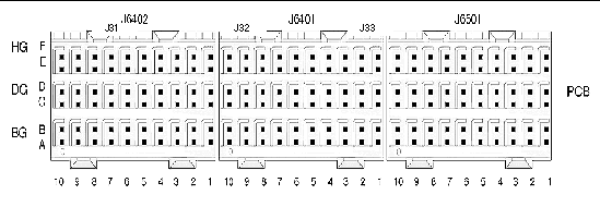
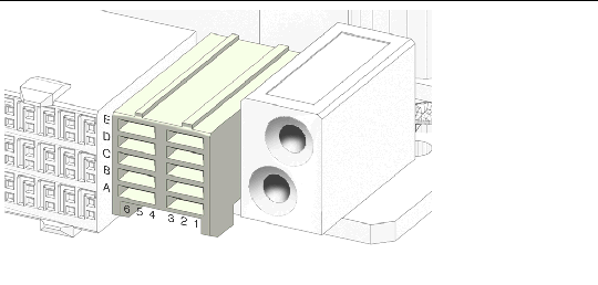
The Netra CP3260 blade server provides all the I/O and power connections for rear access through the Zone 3 RTM connectors. The Zone 3 I/O connectors are shown in FIGURE A-7 and the Zone 3 power connector is shown in FIGURE A-8. The pin numbers and signal assignments are listed in the associated tables.
FIGURE A-7 Zone 3 Signal Connectors

TABLE A-7 gives the Zone 3 J31 connector signals and pin assignments.
TABLE A-7 Zone 3 J31 Connector Pin Assignments
|
Row
|
A
|
B
|
C
|
D
|
E
|
F
|
|
1
|
Z3_F1_TX1+
|
Z3_F1_TX1-
|
Z3_F1_RX0+
|
Z3_F1_RX0-
|
Z3_F1_TX0+
|
Z3_F1_TX0-
|
|
2
|
Z3_F1_RX2+
|
Z3_F1_RX2-
|
Z3_F1_TX2+
|
Z3_F1_TX2-
|
Z3_F1_RX1+
|
Z3_F1_RX1-
|
|
3
|
Z3_F2_TX0+
|
Z3_F2_TX0-
|
Z3_F1_RX3+
|
Z3_F1_RX3-
|
Z3_F1_TX3+
|
Z3_F1_TX3-
|
|
4
|
Z3_F2_RX1+
|
Z3_F2_RX1-
|
Z3_F2_TX1+
|
Z3_F2_TX1-
|
Z3_F2_RX0+
|
Z3_F2_RX0-
|
|
5
|
Z3_F2_TX3+
|
Z3_F2_TX3-
|
Z3_F2_RX2+
|
Z3_F2_RX2-
|
Z3_F2_TX2+
|
Z3_F2_X2-
|
|
6
|
N/U
|
N/U
|
N/U
|
N/U
|
Z3_F2_RX3+
|
Z3_F2_RX3-
|
|
7
|
N/U
|
N/U
|
N/U
|
N/U
|
N/U
|
N/U
|
|
8
|
N/U
|
N/U
|
N/U
|
N/U
|
N/U
|
N/U
|
|
9
|
N/U
|
N/U
|
N/U
|
N/U
|
N/U
|
N/U
|
|
10
|
N/U
|
N/U
|
N/U
|
N/U
|
N/U
|
N/U
|
|
|
|
|
TABLE A-8 gives the Zone 3 J32 connector signals and pin assignments
TABLE A-8 Zone 3 J32 Connector Pin Assignments
|
Row
|
A
|
B
|
C
|
D
|
E
|
F
|
|
1
|
XAUI_MDIO
|
XAUI_MDC
|
N/U
|
N/U
|
N/U
|
N/U
|
|
2
|
N/U
|
N/U
|
N/U
|
N/U
|
SER_RJ45_RTS
|
SER_RJ45_DTR
|
|
3
|
N/U
|
N/U
|
N/U
|
N/U
|
SER_RJ45_TXD
|
SER_RJ45_RXD
|
|
4
|
N/U
|
N/U
|
N/U
|
N/U
|
SER_RJ45_DSR
|
SER_RJ45_CTS
|
|
5
|
N/U
|
N/U
|
N/U
|
N/U
|
N/C
|
N/C
|
|
6
|
RTM_LAN0_A+
|
RTM_LAN0_A-
|
RTM_TXFRMR_
VOLTAGE
|
RTM_TXFRMR_
VOLTAGE
|
RTM_LAN0_B+
|
RTM_LAN0_B-
|
|
7
|
RTM_LAN0_C+
|
RTM_LAN0_C-
|
RTM_ACT_
LED_N
|
RTM_LINK_
LED_N
|
RTM_LAN0_D+
|
RTM_LAN0_D-
|
|
8
|
RTM_SLAN_TX1+
|
RTM_SLAN_
TX1-
|
RTM_SLAN_
RX1+
|
RTM_SLAN_
RX1-
|
N/C
|
N/C
|
|
9
|
RTM_SLAN_TX2+
|
RTM_SLAN_
TX2-
|
RTM_SLAN_
RX2+
|
RTM_SLAN_
RX2-
|
N/U
|
N/U
|
|
10
|
N/U
|
N/U
|
N/U
|
N/U
|
N/U
|
N/U
|
|
|
|
|
TABLE A-9 gives the Zone 3 J33 connector signals and pin assignments.
TABLE A-9 Zone 3 J33 Connector Pin Assignments
|
Row
|
A
|
B
|
C
|
D
|
E
|
F
|
|
1
|
RTM_TX0+
|
RTM_TX0-
|
RTM_RX0+
|
RTM_RX0-
|
RTM_CON_
REF CLK+
|
RTM CON_
REF CLK-
|
|
2
|
RTM_TX1+
|
RTM_TX1-
|
RTM_RX1+
|
RTM_RX1-
|
TCLKA+
|
TCLKA-
|
|
3
|
RTM_TX2+
|
RTM_TX2-
|
RTM_RX2+
|
RTM_RX2-
|
TCLKB+
|
TCLKB-
|
|
4
|
RTM_TX3+
|
RTM_TX3-
|
RTM_RX3+
|
RTM_RX3-
|
TCLKC+
|
TCLKC-
|
|
5
|
RTM_TX4+
|
RTM_TX4-
|
RTM_RX4+
|
RTM_RX4-
|
TCLKD+
|
TCLKD-
|
|
6
|
RTM_TX5+
|
RTM_TX5-
|
RTM_RX5+
|
RTM_RX5-
|
N/U
|
N/U
|
|
7
|
RTM_TX6+
|
RTM_TX6-
|
RTM_RX6+
|
RTM_RX6-
|
N/U
|
N/U
|
|
8
|
RTM_TX7+
|
RTM_TX7-
|
RTM_RX7+
|
RTM_RX7-
|
N/U
|
FPGA_PRESET_
RTM-
|
|
9
|
N/C
|
N/C
|
N/C
|
N/C
|
RTM_MMC_L
|
PCI_CFG
|
|
10
|
N/U
|
N/U
|
N/U
|
N/U
|
GND
|
RTM_CON_EN_L
|
|
|
|
|
FIGURE A-8 Zone 3 Power Connector

TABLE A-10 gives the Zone 3 power connector signals and pin assignments.
TABLE A-10 Zone 3 Power Connector Pin Assignments
|
R
o
w
|
Pin 1
|
Pin 2
|
Pin 3
|
Pin 4
|
Pin 5
|
Pin 6
|
|
A
|
Logic_GND
|
Logic_GND
|
Logic_GND
|
Shelf_GND
|
Shelf_GND
|
Shelf_GND
|
|
B
|
Logic_GND
|
Logic_GND
|
Logic_GND
|
+3.3V_STBY_RTM
|
+3.3V_STBY_RTM
|
+3.3V_STBY_RTM
|
|
C
|
I2C_RTMCONN_SCL
|
I2C_RTMCONN_SCL
|
I2C_RTMCONN_SCL
|
I2C_RTMCONN_SDA
|
I2C_RTMCONN_SDA
|
I2C_RTMCONN_SDA
|
|
D
|
+12V_RTM
|
+12V_RTM
|
+12V_RTM
|
+12V_RTM
|
+12V_RTM
|
+12V_RTM
|
|
E
|
RTM_PS1_L
|
RTM_PS1_L
|
RTM_PS1_L
|
N/C
|
N/C
|
N/C
|
For information about multiplexing to Zone 2 or 3, see Section 4.8, Multiplexing to Zones 2 and 3.
A.4.6 TOD Clock Battery Holder
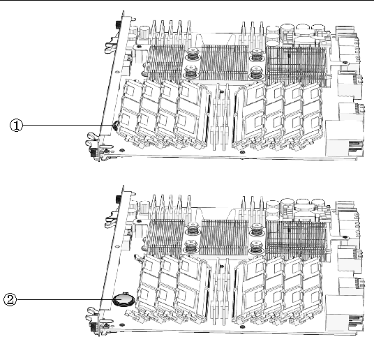
FIGURE A-9 shows the location of the TOD clock battery and holder.
The TOD battery must be type CR1632, with a minimum of 4ma abnormal charging current rating (for example; a Renata CR1632).

|
Caution - Risk of explosion if battery is replaced by an incorrect type.
Dispose of batteries properly in accordance with manufacturer’s instructions and local regulations.
|
To install the battery, slide the battery into the holder with the side labeled “+ “ facing up.
FIGURE A-9 TOD Battery Location

.
Figure Legend
|
1
|
TOD battery location
|
|
2
|
TOD clock battery location with FB-DIMM removed
|
Figure Legend for FIGURE A-9
|
1
|
TOD Battery and Holder
|
| Sun Netra CP3260 Blade Server User’s Guide
|
820-0457-11
|
   
|
Copyright © 2009 Sun Microsystems, Inc. All rights reserved.
