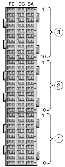
Advanced Rear Transition Module Connectors (Zone 3)
The blade server provides all the I/O connections for rear access through the
Zone 3 ARTM connectors, which support the following:
The J carrier is on the motherboard and a corresponding J carrier is
on the ARTM. Zone 3 connector pins are presented from the point of
view of the ATCA blade, meaning that TX means the ATCA blade is
the signal source, and the ARTM is the signal receiver. Similarly, RX means
the ATCA blade is the signal receiver and the ARTM is the signal
source.
The “reserved” pins indicate connector pins that are currently reserved for compatibility to
all ARTMs. Do not connect signals to reserved pins. The “no connect” indicates pins
that should not be connected by the blade server.
The ARTM Zone 3 connectors are shown in  ARTM Zone 3 Connectors.
For pin assignments of ARTM Zone 3, see the following:
For descriptions of the signals, see  Zone 3 Signal Descriptions.

Figure Legend
1 Zone 3 J33
2 Zone 3 J32
3 Zone 3 J31
Zone 3 Power (J30) Connector Pin Assignments
The J30 connector pin assignments are used for power signals.
|
|
|
|
|
|---|
E |
PS1# |
NC |
Short |
Last |
D |
+12V PP |
+12V
PP |
Long |
First |
C |
IPMI_SCL_L |
IPMI_SDA_L |
Medium |
Second |
B |
Logic_GND |
+3.3V_MP |
Long |
First |
A |
Logic_GND |
Shelf_GND |
Long |
First |
|
Zone 3 AMC I/O (J31) Connector Pin Assignments
The J31 connector pin assignments are used for AMC I/O RTM signals, on
the AMC0 EO interface.
|
|
|
|
|
|
|
|---|
1 |
TX13+ (AMC0 EO_Rx1+) |
TX13- (AMC0 EO_Rx1-) |
GND |
RX12+ (AMC0 EO_Tx0+) |
RX12- (AMC0 EO_Tx0-) |
GND |
TX12+
(AMC0 EO_Rx0+) |
TX12- (AMC0 EO_Rx0-) |
GND |
2 |
RX14+ (AMC0 EO_Tx2+) |
RX14- (AMC0 EO_Tx2-) |
GND |
TX14+ (AMC0 EO_Rx2+) |
TX14- (AMC0 EO_Rx2-) |
GND |
RX13+
(AMC0 EO_Tx1+) |
RX13- (AMC0 EO_Tx1-) |
GND |
3 |
TX17+ (AMC0 EO_Rx4+) |
TX17- (AMC0 EO_Rx4-) |
GND |
RX15+ (AMC0 EO_Tx3+) |
RX15- (AMC0 EO_Tx3-) |
GND |
TX15+
(AMC0 EO_Rx3+) |
TX15- (AMC0 EO_Rx3-) |
GND |
4 |
RX18+ (AMC0 EO_Tx5+) |
RX18- (AMC0 EO_Tx5-) |
GND |
TX18+ (AMC0 EO_Rx5+) |
TX18- (AMC0 EO_Rx5-) |
GND |
RX17+
(AMC0 EO_Tx4+) |
RX17- (AMC0 EO_Tx4-) |
GND |
5 |
TX20+ (AMC0 EO_Rx7+) |
TX20- (AMC0 EO_Rx7-) |
GND |
RX19+ (AMC0 EO_Tx6+) |
RX19- (AMC0 EO_Tx6-) |
GND |
TX19+
(AMC0 EO_Rx6+) |
TX19- (AMC0 EO_Rx6-) |
GND |
6 |
Reserved |
Reserved |
GND |
Reserved |
Reserved |
GND |
RX20+ (AMC0 EO_Tx7+) |
RX20- (AMC0 EO_Tx7-) |
GND |
7 |
Reserved |
Reserved |
GND |
Reserved |
Reserved |
GND |
Reserved |
Reserved |
GND |
8 |
Reserved |
Reserved |
GND |
Reserved |
Reserved |
GND |
Reserved |
Reserved |
GND |
9 |
Reserved |
Reserved |
GND |
Reserved |
Reserved |
GND |
Reserved |
Reserved |
GND |
10 |
Reserved |
Reserved |
GND |
Reserved |
Reserved |
GND |
Reserved |
Reserved |
GND |
|
Zone 3 Infrastructure (J32) Connector Pin Assignments
The J32 connector pin assignments are used for infrastructure signals.
J32 Pin (Infrastructure) Connector Assignments
|
|
|
|
|
|
|
|
|---|
1 |
Reserved |
Reserved |
Reserved |
GND |
Reserved |
Reserved |
GND |
Reserved |
Reserved |
GND |
2 |
SAS AMC0 |
SA TX0+ (AMC0
SAS0_Rx+) |
SA TX0- (AMC0 SAS0_Rx-) |
GND |
SA RX0+ (AMC0 SAS0_Tx+) |
SA RX0- (AMC0 SAS0_Tx-) |
GND |
RTS (Serial 0) |
DTR
(Serial 0) |
GND |
3 |
Reserved |
Reserved |
Reserved |
GND |
Reserved |
Reserved |
GND |
TXD (Serial 0) |
RXD (Serial 0) |
GND |
4 |
SAS AMC0 |
SAS TX2+ (AMC0 SAS1_Rx+) |
SAS TX2- (AMC0
SAS1_Rx+) |
GND |
SAS RX2+ (AMC0 SAS1_Rx+) |
SAS RX2- (AMC0 SAS1_Rx+) |
GND |
DSR (Serial 0) |
CTS (Serial 0) |
GND |
5 |
Reserved |
Reserved |
Reserved |
GND |
Reserved |
Reserved |
GND |
No Connect |
No
Connect |
GND |
6 |
ARTM LAN0 (Mgmt) |
LAN0_A+ |
LAN0_A- |
GND |
LAN0_CTV |
LAN0_CTV |
GND |
LAN0_B+ |
LAN0_B- |
GND |
7 |
ARTM LAN0 (Mgmt) |
LAN0_C+ |
LAN0_C- |
GND |
ACT_LED# |
LINK_LED# |
GND |
LAN0_D+ |
LAN0_D- |
GND |
8 |
ARTM LAN1 (SerDes) |
SLAN_TX1+ |
SLAN_TX1- |
GND |
SLAN_RX1+ |
SLAN_RX1- |
GND |
No Connect |
No Connect |
GND |
9 |
ARTM LAN2 and LAN4
(SerDes) |
SLAN_TX2+ |
SLAN_TX2- |
GND |
SLAN_RX2+ |
SLAN_RX2- |
GND |
No Connect |
No Connect |
GND |
10 |
ARTM LAN3 and LAN4 (SerDes) |
No Connect |
SLAN_TX3- |
GND |
SLAN_RX3+ |
SLAN_RX3- |
GND |
SLAN_RX4+ |
SLAN_RX4- |
GND |
|
Zone 3 PCIe (J33) Connector Pin Assignments
The J33 connector pin assignments are used for PCIe signals.
|
|
|
|
|
|
|
|
|---|
1 |
PCIe x8 Lane |
PETx0+ |
PETx0- |
GND |
PERx0+ |
PERx0- |
GND |
FCLKA+ |
FCLKA- |
GND |
2 |
PCIe x8
Lane |
PETx1+ |
PETx1- |
GND |
PERx1+ |
PERx1- |
GND |
TCLKA+ |
TCLKA- |
GND |
3 |
PCIe x8 Lane |
PETx2+ |
PETx2- |
GND |
PERx2+ |
PERx2- |
GND |
TCLKB+ |
TCLKB- |
GND |
4 |
PCIe x8 Lane |
PETx3+ |
PETx3- |
GND |
PERx3+ |
PERx3- |
GND |
TCLKC+ |
TCLKC- |
GND |
5 |
PCIe x8 Lane |
PETx4+ |
PETx4- |
GND |
PERx4+ |
PERx4- |
GND |
TCLKD+ |
TCLKD- |
GND |
6 |
PCIe x8 Lane |
PETx5+ |
PETx5- |
GND |
PERx5+ |
PERx5- |
GND |
TCK |
TMS |
GND |
7 |
PCIe x8 Lane |
PETx6+ |
PETx6- |
GND |
PERx6+ |
PERx6- |
GND |
TRST# |
TDO |
GND |
8 |
PCIe x8
Lane |
PETx7+ |
PETx7- |
GND |
PERx7+ |
PERx7- |
GND |
TDI |
PCI_RST# |
GND |
9 |
Reserved |
No Connect |
No Connect |
GND |
No Connect |
No Connect |
GND |
ARTM# |
PCI_CFG |
GND |
10 |
Reserved |
No Connect |
No Connect |
GND |
No Connect |
No Connect |
GND |
PS0# |
Enabled# |
GND |
|
Zone 3 Signal Descriptions
 Zone 3 Signal Descriptions provides descriptions of the signals listed in the following Zone 3 pin topics:
Zone 3 Signal Descriptions
|
|
|---|
IPMI_SCL_L |
IPMI bus clock signal, as defined in AMC.0 specification. ARTM has a
pull-up resistor for this signal as indicated in AMC.0 specification. |
IPMI_SDA_L |
IPMI bus data signal,
as defined in AMC.0 specification. ARTM has a pull-up resistor for this signal
as indicated in AMC.0 specification. |
PS0#, PS1# |
Active low ARTM present signal. The PS0# is linked
to logic GND on the ATCA blade, PS1# is pulled up to
3.3V Management Power on the ATCA blade, PS0# and PS1# is connected through diode
on ARTM, exactly as defined in AMC.0 specification. PS1# is last mate on
Power connector and PS0# is on the opposite end of the set of
connectors. Logic low on PS1# indicates that ARTM is present and fully inserted. |
Enable# |
When
low, indicates to ARTM that it is fully inserted and that MMC can
start execution. Logic high keeps MMC in reset state. This signal has a
pull-up resistor as indicated in AMC.0 specification. |
Shelf_GND |
Frame/Chassis Safety Ground. |
Logic_GND |
(Logic 0vdc). Logic Ground-Common return for
Management Power Payload Power, reference potential for single-ended logic signaling, and shielding for
differential pair signals in the AMC connector. |
12VPP |
12V Payload Power, enabled after successful E-keying, following
AMC.0 specification. ARTM meets requirements posted for payload power in AMC specification. |
3.3V_MP |
3.3V Management
Power. ARTM meets requirements posted for management power in AMC.0 specification. |
RX |
AMC Extended Options
receive differential pair signals. Note that this specification takes ATCA blade perspective, which means
that RX signals are driven by ARTM and received by ATCA blade. |
TX |
AMC Extended
Options transmit differential pair signals. Note that this specification takes ATCA blade perspective, which
means that TX signals are driven by ATCA blade and received by ARTM. |
SA_TX |
SAS
or SATA transmit differential pair signals. |
SA_RX |
SAS or SATA receive differential pair signals. |
Serial 0 |
RS-232 Serial
Signals, Transmit, Receive, Clear to Send, Request to Send, Data Terminal Ready, and
Data Set Ready. |
LAN0 |
10/100/1000BASE-T signals. |
LAN0_CTV |
10/100/1000BASE-T transformer Center Tap signal, which could be used to terminate
center tap of transformers placed on the ARTM. This signal is applicable if
Ethernet PHY is located on ATCA blade, while transformers are located on ARTM. |
ACT_LED# |
LAN
0 (Management) activity indicator signal for LED (active low). |
LINK_LED# |
LAN 0 (Management) LINK indicator
signal for LED (active low). |
PCI_CFG |
PCI Express bus configuration signal. It must be grounded on
ARTMs that use a single x8 PCI Express bus and pulled up on
the ATCA with 10Kohm resistor to management power. On ARTMs that expect two
x4 PCI-Express buses, this pin will float (not be connected). Two x4 PCI-Express
buses are intended for ARTM implementations that desire to avoid PCI-Express switch in
order to reduce latency. |
ARTM# |
ARTM# signal must be grounded on ARTMs that implement MMC controller
as defined by AMC.0 specification. This signal is pulled up with 10Kohm resistor
to management power on the ATCA node blade server. |
SLAN_TX |
GBEthernet SerDes transmit differential pair signals. |
SLAN_RX |
GBEthernet
SerDes receive differential pair signals. |
PETx |
PCI-Express transmit differential pair signals. |
PERx |
PCI-Express receive differential pair signals. |
PCI_RST# |
PCI-Express reset signal.
Logic low resets downstream PCI-Express devices on ARTM. |
TCLKA |
PCI-Telecom clock A 19.44MHz, differential pair into
ARTM (ATCA CLK2) as defined in AMC.0 specification. |
TCLKB |
PCI-Telecom clock B 19.44MHz, differential pair
out from ARTM (ATCA CLK3) as defined in AMC.0 specification. |
TCLKC |
PCI-Telecom clock C
8kHz, differential pair into ARTM (ATCA CLK1) as defined in AMC.0 specification. |
TCLKD |
PCI-Telecom clock
D 8kHz, differential pair out from ARTM as defined in AMC.0 specification. |
FCLKA |
Fabric clock,
as defined in AMC.0 specification. Intended to be used for PCI-Express 100 MHz
spread spectrum clock. |
TCK, TMS, TRST#, TDO, TDI |
JTAG signals. Signal direction follows AMC.0 specification. |
|

![]() ARTM Zone 3 Connectors.
ARTM Zone 3 Connectors.![]() Zone 3 Signal Descriptions.
Zone 3 Signal Descriptions.
![]() Zone 3 Signal Descriptions provides descriptions of the signals listed in the following Zone 3 pin topics:
Zone 3 Signal Descriptions provides descriptions of the signals listed in the following Zone 3 pin topics: