This appendix contains information about the following connector pinouts:
C.1 Front I/O Dongle
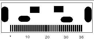
The front I/O dongle connector pins and their corresponding descriptions are shown in the figure and table in this section.
FIGURE C-1 Front I/O Dongle Connector

TABLE C-1 Front I/O Dongle Pins
|
Signal Name
|
Pin #
|
Pin #
|
Signal Name
|
|
No Connect
|
1, 21, 28, 30, 31, 33, 34
|
15
|
USB0_FRONT_VCC
|
|
DNGL_VGA_RED
|
2
|
16
|
USB1_FRONT_VCC
|
|
DNGL_VGA_GRN
|
3
|
17
|
USB1_FRONT_VCC
|
|
DNGL_VGA_BLU
|
4
|
18
|
USB1_FRONT_CM_N
|
|
GND
|
5
|
19
|
USB1_FRONT_CM_P
|
|
DNGL_VGA_MONID2
|
6
|
20
|
GND
|
|
GND
|
7, 11, 20, 29, 32, 36
|
22
|
DNGL_RES_SER_RXD
|
|
DNGL_VGA_MONID1
|
8
|
23
|
RES_DNGL_SER_RTS_N
|
|
DNGL_VGA_HSYNC_BUF
|
9
|
24
|
RES_DNGL_SER_TXD
|
|
DNGL_VGA_VSYNC_BUF
|
10
|
25
|
DNGL_RES_SER_CTS_N
|
|
GND
|
11
|
26
|
RES_DNGL_SER_DTR_N
|
|
USB0_FRONT_CM_N
|
12
|
27
|
DNGL_RES_SER_DCD_N
|
|
USB0_FRONT_CM_P
|
13
|
35
|
DONGLE_PRSNT_L
|
|
USB0_FRONT_VCC
|
14
|
|
|
C.2 SAS/SATA Connectors
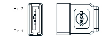
The Serial Attached SCSI (SAS)/Serial Advanced Technology Attachment (SATA) connector pins and their corresponding descriptions are shown in the figure and table in this section.
FIGURE C-2 SAS/SATA Connector

TABLE C-2 SAS/SATA Connector Pins
|
Segment
|
Pin Number
|
Pin Name
|
Description
|
|
Signal Segment
|
S1
|
Gnd
|
Second mate ground
|
|
S2
|
TX+
|
Positive side of transmit to hard drive
|
|
S3
|
TX-
|
Negative side of transmit to hard drive
|
|
S4
|
Gnd
|
Second mate ground
|
|
S5
|
RX-
|
Negative side of receive from hard drive
|
|
S6
|
RX+
|
Positive side of receive from hard drive
|
|
S7
|
Gnd
|
Second mate ground
|
|
Backside Signal Segment
|
S8
|
Gnd
|
Second mate ground
|
|
S9
|
|
Not used
|
|
S10
|
|
Not used
|
|
S11
|
Gnd
|
Second mate ground
|
|
S12
|
|
Not used
|
|
S13
|
|
Not used
|
|
S14
|
Gnd
|
Second mate ground
|
|
Power Segment
|
P1
|
3.3 V
|
Not used
|
|
P2
|
3.3 V
|
Not used
|
|
P3
|
3.3 V
|
Not used
|
|
P4
|
Gnd
|
First mate ground
|
|
P5
|
Gnd
|
Second mate ground
|
|
P6
|
Gnd
|
Second mate ground
|
|
P7
|
5.0 V
|
Pre-charge, second mate
|
|
P8
|
5.0 V
|
|
|
P9
|
5.0 V
|
|
|
P10
|
Gnd
|
Second mate ground
|
|
P11
|
Reserved
|
Should be grounded
|
|
P12
|
Gnd
|
First mate ground
|
|
P13
|
12.0 V
|
Pre-charge, second mate
|
|
P14
|
12.0 V
|
|
|
P15
|
12.0 V
|
|
C.3 SAS Diskplane
The SAS diskplane connector pins and their corresponding descriptions are shown in the figure and table in this section.
FIGURE C-3 SAS Diskplane Signal Connector

TABLE C-3 SAS Disk Backplane Signal Connector Pins
|
Pin Number
|
Signal Name
|
|
1, 4, 7
|
GND
|
|
2, 3
|
TX+/TX-
|
|
5, 6
|
RX+/RX-
|
C.4 SAS Power/LED Connector
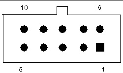
The SAS power/LED connector pins and their corresponding descriptions are shown in the figure and table in this section.
FIGURE C-4 SAS Power/LED Connector

TABLE C-4 SAS Power/LED Connector Pins
|
Pin Number
|
Signal Name
|
|
1
|
DISK1_FAULT_LED_L
|
|
2
|
DISK1_RDY2RM_L
|
|
3
|
DISK1_PRSNT_L
|
|
4
|
12V
|
|
5
|
GND
|
|
6
|
DISK0_FAULT_LED_L
|
|
7
|
DISK0_RDY2RM_L
|
|
8
|
DISK0_PRSNT_L
|
|
9
|
GND
|
|
10
|
5V
|
C.5 Compact Flash
The Compact Flash connector pins and their corresponding descriptions are shown in the figure and table in this section.

FIGURE C-5 Compact Flash Connector
TABLE C-5 Compact Flash Connector Pins
|
Signal Name
|
Pin #
|
Pin #
|
Signal Name
|
|
GND
|
1
|
26
|
PRSNT_N
|
|
D03
|
2
|
27
|
D11
|
|
D04
|
3
|
28
|
D12
|
|
D05
|
4
|
29
|
D13
|
|
D06
|
5
|
30
|
D14
|
|
D07
|
6
|
31
|
D15
|
|
CS1_L
|
7
|
32
|
CS3_L
|
|
GND
|
8
|
33
|
No Connect
|
|
ATA_SEL
|
9
|
34
|
IOR_L
|
|
GND
|
10
|
35
|
IOW_L
|
|
GND
|
11
|
36
|
WE
|
|
GND
|
12
|
37
|
INT_L
|
|
3.3V
|
13
|
38
|
3.3V
|
|
GND
|
14
|
39
|
IDE_CSEL
|
|
GND
|
15
|
40
|
No Connect
|
|
GND
|
16
|
41
|
IDE_RESET_L
|
|
GND
|
17
|
42
|
IDE_RDY
|
|
ADDR2
|
18
|
43
|
DRQ_L
|
|
ADDR1
|
19
|
44
|
DACK_L
|
|
ADDR0
|
20
|
45
|
No Connect
|
|
D00
|
21
|
46
|
No Connect
|
|
D01
|
22
|
47
|
D08
|
|
D02
|
23
|
48
|
D09
|
|
No Connect
|
24
|
47
|
D10
|
|
IDE_CD2
|
15
|
50
|
GND
|
| Sun Blade X6240 Server Module Service Manual
|
820-3971-11
|
    |
Copyright © 2009 Sun Microsystems, Inc. All rights reserved.
