C.1.4 Memory System
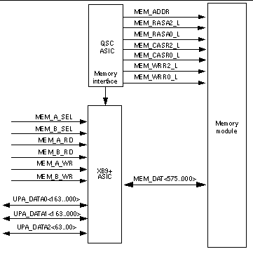
The memory system consists of three components: the QSC ASIC, the XB9+ ASIC, and the memory module. The QSC ASIC generates memory addresses and control signals to the memory module. The QSC ASIC also coordinates the data transfers among the DIMMs through two 144-bit-wide processor data buses (UPA_DATABUS0) and the 72-bit-wide I/O data bus (UPA_DATABUS1).
DIMMs are organized in banks in groups of four (quads). DIMM capacities of 32-Mbyte, 64-Mbyte, and 128-Mbyte are supported by the memory module. When all DIMM banks are populated with 128-Mbyte DIMMs, maximum memory capacity is 2 Gbytes.
Organizing the four DIMM banks with 128-Mbyte (plus ECC bit) DIMMs allows data streams to be transferred on a 512-bit-wide (plus ECC) memory data bus. The XB9+ ASIC coordinates all buses, which include the following: memory data, UPA_DATA0, UPA_DATA1, UPA_DATA2, and UPA_DATA3.
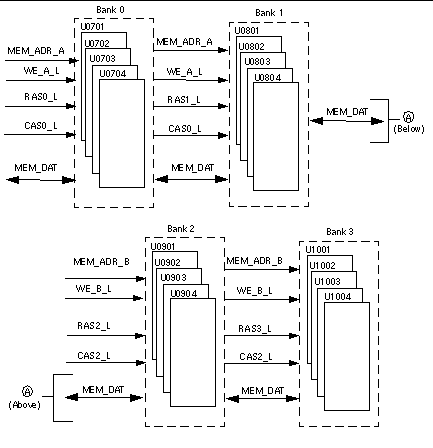
The memory module is arranged in four banks. DIMMs are always accessed four at a time. Consequently, the DIMMs must be installed in groups of four (quad) and individual DIMMs within a bank must be of equal capacity.
The following figure illustrates the memory module functional block diagram.

Failure to populate a DIMM bank with DIMMs of equal capacity will result in inefficient use of memory resource or system failure.
The following figure shows the system memory functional block diagram.
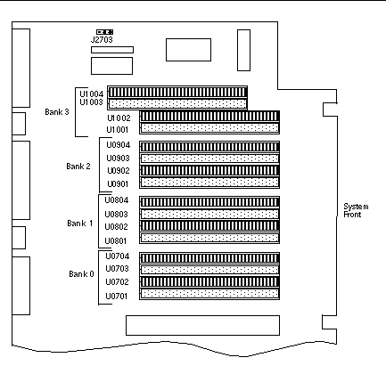
The following figure shows system memory bank locations and addresses on the main logic board.
C.1.4.1 DIMM
The DIMM is a 60-nanosecond, fast-page-mode-style DIMM. Three DIMM configurations are supported in the system unit: 32-Mbyte, 64-Mbyte, and 128-Mbyte. The minimum memory capacity is 128 Mbytes (four 32-Mbyte DIMMs). The maximum memory capacity is 2 Gbytes (sixteen 128-Mbyte DIMMs).
A block of data (64 bytes) always comes from one bank of DIMMs. An error code containing the address of where a failure occurred, as well as the associated syndrome, is logged when an ECC error occurs.
There are a total of four DIMM banks in the system unit.
|
DIMM Bank |
U Number |
|
0 |
U0701 through U0704 |
|
1 |
U0801 through U0804 |
|
2 |
U0901 through U0904 |
|
3 |
U1001 through U1004 |
|
DIMM Bank |
PA[30:28] |
|
0 |
0000 |
|
|
0001 |
|
1 |
0010 |
|
|
0011 |
|
2 |
1000 |
|
|
1001 |
|
3 |
1010 |
|
|
1011 |
C.1.4.2 Memory System Timing
The QSC ASIC generates the memory addresses and control signals to the memory system. The UPA clock is the clock source for the QSC ASIC and operates as fast as 120 MHz.
- © 2010, Oracle Corporation and/or its affiliates
