Specifications for the Sun Netra CP3060 blade server are provided in the following sections:
A.1 Form Factor
The Sun Netra CP3060 blade server is a standard 8U form factor, a single-slot-wide. It complies with the board mechanical dimensions required by the PICMG 3.0 R1.0 Specification:
- 322.25 mm x 280 mm (length x width)
- 1.2-inch-wide front panel
A.2 Layout
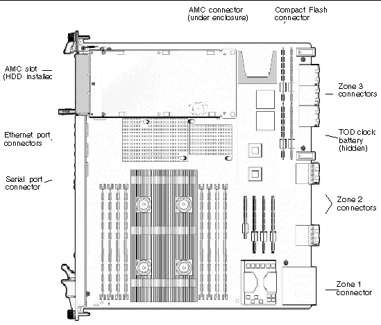
The Sun Netra CP3060 blade server layout is shown in FIGURE A-1.
FIGURE A-1 Sun Netra CP3060 Blade Server Layout
A.3 Front Panel
The single-slot-wide, 8U front panel was designed to meet PICMG 3.0 R 1.0 and other specifications.
A.3.1 Visual Indicators
The Sun Netra CP3060 blade server has the following indicators on the front panel:
- Green LED - Blade Server’s healthy status or user programmable (ACTIVE).
- Amber LED - Blade Server’s fault condition (FAULT).
- Blue LED - Indicates safe removal (hot-swap activity).
The front panel’s Ethernet ports do not have LED indicators.
A.3.2 Ports
The Sun Netra CP3060 blade server has the following ports on the front panel:
- One serial port (RJ-45)
- Two 10/100/1000BASE-T Ethernet ports (RJ-45)
A.3.3 AMC Slot
The Netra CP3060 blade server has an AMC I/O full-height, single-width slot that is accessable through the AMC cutout on the front panel.
A.4 Connectors and Pinout
FIGURE A-1 shows all the basic I/O connectors to the front and the rear of the Sun Netra CP3060 blade server.
A.4.1 Front Panel Connectors
The front panel has the following connectors:
- Two 10/100/1000BASE-T Ethernet ports (RJ-45)
- One serial port (RJ-45)
- AMC connector (via AMC slot)
A.4.1.1 Ethernet Ports
The Ethernet connectors are RJ-45 connectors. The controller autonegotiates to either 10BASE-T,100BASE-T, or 1000BASE-T. The Ethernet connector pin numbering is shown in FIGURE A-2.
FIGURE A-2 Ethernet RJ-45 Connector
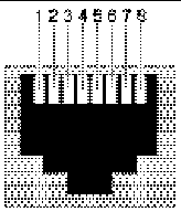
TABLE A-1 shows the Ethernet connector pin assignments. The 1000BASE-T signal names are in parentheses.
TABLE A-1 Ethernet Port Connector Pin Assignments
|
Pin
|
Signal Name
|
Pin
|
Signal Name
|
|
1
|
TXD+
|
(BI_DA+)
|
5
|
not used
|
(BI_DC-)
|
|
2
|
TXD-
|
(BI_DA-)
|
6
|
RXD-
|
(BI_DB-)
|
|
3
|
RXD+
|
(BI_DB+)
|
7
|
not used
|
(BI_DD+)
|
|
4
|
not used
|
(BI_DC+)
|
8
|
not used
|
(BI_DD-)
|
A.4.1.2 Serial Port
FIGURE A-3 contains the connector pin assignments for the front panel serial port.
FIGURE A-3 Front Panel Serial Port Diagram

TABLE A-2 shows the serial port connector pin assignments.
TABLE A-2 Serial Port RJ-45 Connector Pinouts
|
Pin
|
Signal Name
|
Pin
|
Signal Name
|
|
1
|
RTS
|
5
|
DCD
|
|
2
|
DTR
|
6
|
RXD
|
|
3
|
TXD
|
7
|
DSR
|
|
4
|
GND
|
8
|
CTS
|
A.4.2 AMC Connector
The Sun Netra CP3060 blade server provides a B+ style 170-pin connector. The pinout of the AMC slot is provided in TABLE A-3.
- The signals denoted RTM are wired to the Zone 3 RTM connector. (These are port 12 through port 20 in the AMC specification, part of the Extended Options Region.)
- The signals denoted PCI-E are connected with an x8 port on the PCI-E switch. (These are port 4 through port 11 in the AMC specification, part of the Fabric I/O Region.)
- The signals denoted SATA are wired to two of the SATA controller ports. (These are port 2 and port 3 in the AMC specification, part of the Common Options Region.)
TABLE A-3 AMC Connector Pin Assignments
|
Basic Side
|
Extended Side
|
Basic Side
|
Extended Side
|
|
Pin
|
Signal
|
Pin
|
Signal
|
Pin
|
Signal
|
Pin
|
Signal
|
|
85
|
Gnd
|
86
|
Gnd
|
42
|
12V
|
129
|
RTM_TX3_N
|
|
84
|
12V
|
87
|
PCIE_RX4_N
|
41
|
AMC_CONN_ENABLE_L
|
130
|
RTM_TX3_P
|
|
83
|
Gnd
|
88
|
PCIE_RX4_P
|
40
|
Gnd
|
131
|
Signal
|
|
82
|
Gnd
|
89
|
Gnd
|
39
|
SATA1_AMC_TX_N
|
132
|
RTM_RX3_N
|
|
81
|
AMCCON_REFCLK_N
|
90
|
PCIE_TX4_N
|
38
|
SATA1_AMC_TX_P
|
133
|
RTM_RX3_P
|
|
80
|
AMCCON_REFCLK_P
|
91
|
PCIE_TX4_P
|
37
|
Gnd
|
134
|
Gnd
|
|
79
|
Gnd
|
92
|
Gnd
|
36
|
SATA1_AMC_RXX_N
|
135
|
RTM_TX4_N
|
|
78
|
CLK2_N
|
93
|
PCIE_RX5_N
|
35
|
SATA1_AMC_RXX_P
|
136
|
RTM_TX4_P
|
|
77
|
CLK2_P
|
94
|
PCIE_RX5_P
|
34
|
Gnd
|
137
|
Gnd
|
|
76
|
Gnd
|
95
|
Gnd
|
33
|
SATA0_AMC_TX_N
|
138
|
RTM_RX4_N
|
|
75
|
CLK1_N
|
96
|
PCIE_TX5_N
|
32
|
SATA0_AMC_TX_P
|
139
|
RTM_RX4_P
|
|
74
|
CLK1_P
|
97
|
PCIE_TX5_P
|
31
|
Gnd
|
140
|
Gnd
|
|
73
|
Gnd
|
98
|
Gnd
|
30
|
SATA0_AMC_RXX_N
|
141
|
RTM_TX5_N
|
|
72
|
12V
|
99
|
PCIE_RX6_N
|
29
|
SATA0_AMC_RXX_P
|
142
|
RTM_TXx5_P
|
|
71
|
I2C_AMCCONN_SDA
|
100
|
PCIE_RX6_P
|
28
|
Gnd
|
143
|
Gnd
|
|
70
|
Gnd
|
101
|
Gnd
|
27
|
12V
|
144
|
RTM_RX5_N
|
|
69
|
PCIE_RX3_N
|
102
|
PCIE_TX6_N
|
26
|
Gnd
|
145
|
RTM_RX5_P
|
|
68
|
PCIE_RX3_P
|
103
|
PCIE_TX6_P
|
25
|
Gnd
|
146
|
Gnd
|
|
67
|
Gnd
|
104
|
Gnd
|
24
|
n/c
|
147
|
RTM_TX6_N
|
|
66
|
PCIE_TX3_N
|
105
|
PCIE_RX7_N
|
23
|
n/c
|
148
|
RTM_TX6_P
|
|
65
|
PCIE_TX3_P
|
106
|
PCIE_RX7_P
|
22
|
Gnd
|
149
|
Gnd
|
|
64
|
Gnd
|
107
|
Gnd
|
21
|
n/c
|
150
|
RTM_RX6_N
|
|
63
|
PCIE_RX2_N
|
108
|
PCIE_TX7_N
|
20
|
n/c
|
151
|
RTM_RX6_P
|
|
62
|
PCIE_RX2_P
|
109
|
PCIE_TX7_P
|
19
|
Gnd
|
152
|
Gnd
|
|
61
|
Gnd
|
110
|
Gnd
|
18
|
12V
|
153
|
RTM_TX7_N
|
|
60
|
PCIE_TX2_N
|
111
|
RTM_TX0_N
|
17
|
Gnd
|
154
|
RTM_TX7_P
|
|
59
|
PCIE_TX2_P
|
112
|
RTM_TX0_P
|
16
|
Gnd
|
155
|
Gnd
|
|
58
|
Gnd
|
113
|
Gnd
|
15
|
n/c
|
156
|
RTM_RX7_N
|
|
57
|
12V
|
114
|
RTM_RX0_N
|
14
|
n/c
|
157
|
RTM_RX7_P
|
|
56
|
I2C_AMCCONN_SCL
|
115
|
RTM_RX0_P
|
13
|
Gnd
|
158
|
Gnd
|
|
55
|
Gnd
|
116
|
Gnd
|
12
|
n/c
|
159
|
RTM_TX8_N
|
|
54
|
PCIE_RX1_N
|
117
|
RTM_TX1_N
|
11
|
n/c
|
160
|
RTM_TX8_P
|
|
53
|
PCIE_RX1_P
|
118
|
RTM_TX1_P
|
10
|
Gnd
|
161
|
Gnd
|
|
52
|
Gnd
|
19
|
Gnd
|
9
|
12V
|
162
|
RTM_RX8_N
|
|
51
|
PCIE_TX1_N
|
120
|
RTM_RX1_N
|
8
|
nGnd
|
163
|
RTM_RX8_P
|
|
50
|
PCIE_TX1_N
|
121
|
RTM_RX1_P
|
7
|
Gnd
|
164
|
Gnd
|
|
49
|
Gnd
|
122
|
Gnd
|
6
|
Gnd
|
165
|
TCLK
|
|
48
|
PCIE_RX0_N
|
123
|
RTM_TX2_N
|
5
|
n/c
|
166
|
TMS
|
|
47
|
PCIE_RX0_P
|
124
|
RTM_TX2_P
|
4
|
3.3v_AMC
|
167
|
TRST
|
|
46
|
Gnd
|
125
|
Gnd
|
3
|
AMC_PS1_L
|
168
|
TDO
|
|
45
|
PCIE_TX0_N
|
126
|
RTM_RX2_N
|
2
|
12V
|
169
|
TDI
|
|
44
|
PCIE_TX0_P
|
127
|
RTM_RX2_P
|
1
|
Gnd
|
170
|
Gnd
|
|
43
|
Gnd
|
128
|
Gnd
|
|
|
|
|
A.4.3 Compact Flash Connector
The Compact Flash connector is a type I/II connector.
A.4.4 Midplane Power Connector (Zone 1)
The Sun Netra CP3060 blade server uses a Zone 1 power connector. It provides support for the following signals:
- Two -48 volt DC power feeds (four signals each; eight signals total)
- Two IPMB ports (two signals each, four signals total)
- Geographic address (eight signals)
The analog test and ring voltage pins are left unconnected.
FIGURE A-4 shows the pin assignments.
FIGURE A-4 Power Distribution Connector (Zone 1) P10

TABLE A-4 lists the power connector pin assignments.
TABLE A-4 Power Distribution Connector Pin Assignments
|
Pin Number
|
Name
|
Description
|
|
1
|
Reserved
|
Reserved
|
|
2
|
Reserved
|
Reserved
|
|
3
|
Reserved
|
Reserved
|
|
4
|
Reserved
|
Reserved
|
|
5
|
HA0
|
HA0 Hardware Address Bit 0
|
|
6
|
HA1
|
HA1 Hardware Address Bit 1
|
|
7
|
HA2
|
HA2 Hardware Address Bit 2
|
|
8
|
HA3
|
HA3 Hardware Address Bit 3
|
|
9
|
HA4
|
HA4 Hardware Address Bit 4
|
|
10
|
HA5
|
HA5 Hardware Address Bit 5
|
|
11
|
HA6
|
HA6 Hardware Address Bit 6
|
|
12
|
HA7/P
|
HA7/P Hardware Address Bit 7(Odd Parity Bit)
|
|
13
|
SCL_A
|
IPMB Clock, Port A
|
|
14
|
SDA_A
|
IPMB Data, Port A
|
|
15
|
SCL_B
|
IPMB Clock, Port B
|
|
16
|
SDA_B
|
IPMB Data, Port B
|
|
17
|
Unused
|
|
|
18
|
Unused
|
|
|
19
|
Unused
|
|
|
20
|
Unused
|
|
|
21
|
Unused
|
|
|
22
|
Unused
|
|
|
23
|
Unused
|
|
|
24
|
Unused
|
|
|
25
|
SHELF_GND
|
Shelf Ground
|
|
26
|
LOGIC_GND
|
Logic Ground
|
|
27
|
ENABLE_B
|
Enable B
|
|
28
|
VRTN_A
|
Voltage Return A
|
|
29
|
VRTN_B
|
Voltage Return B
|
|
30
|
EARLY_A
|
-48V Early A
|
|
31
|
EARLY_B
|
-48V Early B
|
|
32
|
ENABLE_A
|
Enable A
|
|
33
|
-48V_A
|
-48V A
|
|
34
|
-48V_B
|
-48V B
|
A.4.5 Data Transport Connector (Zone 2)
The data transport connector consists of one 120-pin HM-Zd connector, labeled P23, with 40 differential pairs. This is called the Zone 2 connector.
The Zone 2 connector provides the following signals:
- Two 1000BASE-T Ethernet Base Fabric channels
- Two 1000 SERDES ports on the Extended Fabric interface
- Synchronization Clock interface supporting CLK1A/B and CLK2A/2B
FIGURE A-5 shows the Zone 2 connectors.
FIGURE A-5 Zone 2 Connectors

TABLE A-5 gives the Zone 2 J10101 connector pin assignments.
TABLE A-5 Zone 2 J10101 Connector Pin Assignments
|
Row
|
A
|
B
|
C
|
D
|
E
|
F
|
G
|
H
|
|
1
|
n/c
|
n/c
|
P23_F2_
TERM_RX2+
|
P23_F2_
TERM_RX2-
|
n/c
|
/c
|
P23_F2_
TERM_RX3+
|
P2_F2_
TERM_RX3+
|
|
2
|
GBE_EXTB_TX0_P
|
GBE_EXTB_TX0_N
|
GBE_EXTB_RX0_P
|
GBE_EXTB_RX0_N
|
n/c
|
n/c
|
P23_F2_
TERM_RX1+
|
P23_F2_
TERM_RX1+
|
|
3
|
n/c
|
n/c
|
P23_F1_
TERM_RX2+
|
P23-F1_
TERM_RX2+
|
n/c
|
n/c
|
P23_F1_
TERM_RX3+
|
P23_F1_
TERM_RX3+
|
|
4
|
GBE_EXTA_TX0_P
|
GBE_EXTA_TX0_N
|
GBE_EXTA_RX0_P
|
GBE_EXTA_RX0_N
|
n/c
|
n/c
|
P23_F1_
TERM_RX1+
|
P23_F1_
TERM_RX1+
|
|
5
|
GBE_BASE_
Z2A_TR0_P
|
GBE_BASE_
Z2A_TR0_N
|
GBE_BASE_
Z2A_TR1_P
|
GBE_BASE_
Z2A_TR1_N
|
GBE_BASE_
Z2A_TR2_P
|
GBE_BASE_
Z2A_TR2_N
|
GBE_BASE_
Z2A_TR3_P
|
GBE_BASE_
Z2A_TR3_N
|
|
6
|
GBE_BASE_
Z2B_TR0_P
|
GBE_BASE_
Z2B_TR0_N
|
GBE_BASE_
Z2B_TR1_P
|
GBE_BASE_
Z2B_TR1_N
|
GBE_BASE_
Z2B_TR2_P
|
GBE_BASE_
Z2B_TR2_N
|
GBE_BASE_
Z2B_TR3_P
|
GBE_BASE_
Z2B_TR3_N
|
|
7
|
n/c
|
n/c
|
n/c
|
n/c
|
n/c
|
n/c
|
n/c
|
n/c
|
|
8
|
n/c
|
n/c
|
n/c
|
n/c
|
n/c
|
n/c
|
n/c
|
n/c
|
|
9
|
n/c
|
n/c
|
n/c
|
n/c
|
n/c
|
n/c
|
n/c
|
n/c
|
|
10
|
n/c
|
n/c
|
n/c
|
n/c
|
n/c
|
n/c
|
n/c
|
n/c
|
TABLE A-6 gives the Zone 2 J10001 connector pin assignments.
TABLE A-6 Zone 2 J10001 Connector Pin Assignments
|
Row
|
A
|
B
|
C
|
D
|
E
|
F
|
G
|
H
|
|
1
|
Clk1A_P
|
Clk1A_N
|
Clk1B_P
|
Clk1B_N
|
Clk2A_P
|
Clk2A_N
|
Clk2B_P
|
Clk2B_n
|
|
2
|
n/c
|
n/c
|
n/c
|
n/c
|
n/c
|
n/c
|
n/c
|
n/c
|
|
3
|
n/c
|
n/c
|
n/c
|
n/c
|
n/c
|
n/c
|
n/c
|
n/c
|
|
4
|
n/c
|
n/c
|
n/c
|
n/c
|
n/c
|
n/c
|
n/c
|
n/c
|
|
5
|
n/c
|
n/c
|
n/c
|
n/c
|
n/c
|
n/c
|
n/c
|
n/c
|
|
6
|
n/c
|
n/c
|
n/c
|
n/c
|
n/c
|
n/c
|
n/c
|
n/c
|
|
7
|
n/c
|
n/c
|
n/c
|
n/c
|
n/c
|
n/c
|
n/c
|
n/c
|
|
8
|
n/c
|
n/c
|
n/c
|
n/c
|
n/c
|
n/c
|
n/c
|
n/c
|
|
9
|
n/c
|
n/c
|
n/c
|
n/c
|
n/c
|
n/c
|
n/c
|
n/c
|
|
10
|
n/c
|
n/c
|
n/c
|
n/c
|
n/c
|
n/c
|
n/c
|
n/c
|
A.4.6 RTM Connector (Zone 3)
The Sun Netra CP3060 blade server provides all the I/O connections for rear access through the Zone 3 RTM connector. The connector view and the pinouts for the Zone 3 connectors are shown in FIGURE A-6.
FIGURE A-6 Zone 3 Connectors
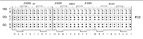
TABLE A-7 gives the Zone 3 J10202 connector pin assignments.
TABLE A-7 Zone 3 J10202 Connector Pin Assignments
|
Row
|
A
|
B
|
BG
|
C
|
D
|
DG
|
E
|
F
|
FG
|
|
1
|
PCIE_Tx7_p
|
PCIE_Tx7_n
|
GND
|
PCIE_Rx7_p
|
PCIE_Rx7_n
|
GND
|
n/c
|
n/c
|
GND
|
|
2
|
PCIE_Tx6_p
|
PCIE_Tx6_n
|
GND
|
PCIE_Rx6_p
|
PCIE_Rx6_n
|
GND
|
n/c
|
n/c
|
GND
|
|
3
|
PCIE_Tx5_p
|
PCIE_Tx5_n
|
GND
|
PCIE_Rx5_p
|
PCIE_Rx5_n
|
GND
|
n/c
|
n/c
|
GND
|
|
4
|
PCIE_Tx4_p
|
PCIE_Tx4_n
|
GND
|
PCIE_Rx4_p
|
PCIE_Rx4_n
|
GND
|
n/c
|
n/c
|
GND
|
|
5
|
PCIE_Tx3_p
|
PCIE_Tx3_n
|
GND
|
PCIE_Rx3_p
|
PCIE_Rx3_n
|
GND
|
n/c
|
n/c
|
GND
|
|
6
|
PCIE_Tx2_p
|
PCIE_Tx2_n
|
GND
|
PCIE_Rx2_p
|
PCIE_Rx2_n
|
GND
|
n/c
|
n/c
|
GND
|
|
7
|
PCIE_Tx1_p
|
PCIE_Tx1_n
|
GND
|
PCIE_Rx1_p
|
PCIE_Rx1_n
|
GND
|
n/c
|
n/c
|
GND
|
|
8
|
PCIE_Tx0_p
|
PCIE_Tx0_n
|
GND
|
PCIE_Rx0_p
|
PCIE_Rx0_n
|
GND
|
n/c
|
n/c
|
GND
|
|
9
|
n/c
|
n/c
|
GND
|
n/c
|
n/c
|
GND
|
n/c
|
n/c
|
GND
|
|
10
|
n/c
|
n/c
|
GND
|
n/c
|
n/c
|
GND
|
n/c
|
n/c
|
GND
|
TABLE A-8 gives the Zone 3 J10201 connector pin assignments.
TABLE A-8 Zone 3 J10201 Connector Pin Assignments
|
Row
|
A
|
B
|
BG
|
C
|
D
|
DG
|
E
|
F
|
FG
|
|
1
|
AMC0_IO1
|
AMC0_IO2
|
|
AMC0_IO3
|
AMC0_IO4
|
|
AMC0_IO5
|
AMC0_IO6
|
GND
|
|
2
|
AMC0_IO7
|
AMC0_IO8
|
|
AMC0_IO9
|
AMC0_IO10
|
|
AMC0_IO11
|
AMC0_IO12
|
|
|
3
|
AMC0_IO24
|
AMC0_IO23
|
|
AMC0_IO22
|
AMC0_IO21
|
|
AMC0_IO20
|
AMC0_IO19
|
|
|
4
|
AMC0_IO18
|
AMC0_IO17
|
|
AMC0_IO16
|
AMC0_IO15
|
GND
|
AMC0_IO14
|
AMC0_IO13
|
|
|
5
|
AMC0_IO36
|
AMC0_IO35
|
GND
|
AMC0_IO34
|
AMC0_IO33
|
|
AMC0_IO32
|
AMC0_IO31
|
|
|
6
|
AMC0_IO30
|
AMC0_IO29
|
|
AMC0_IO28
|
AMC0_IO27
|
|
AMC0_IO26
|
AMC0_IO25
|
GND
|
|
7
|
n/c
|
n/c
|
|
n/c
|
n/c
|
|
n/c
|
n/c
|
|
|
8
|
n/c
|
n/c
|
|
n/c
|
n/c
|
|
n/c
|
n/c
|
|
|
9
|
n/c
|
n/c
|
|
n/c
|
n/c
|
|
n/c
|
n/c
|
|
|
10
|
n/c
|
n/c
|
|
n/c
|
n/c
|
|
n/c
|
n/c
|
|
TABLE A-9 gives the Zone 3 J10301 connector pin assignments.
TABLE A-9 Zone 3 J10301 Connector Pin Assignments
|
Row
|
A
|
B
|
BG
|
C
|
D
|
DG
|
E
|
F
|
FG
|
|
1
|
n/c
|
n/c
|
|
n/c
|
n/c
|
|
n/c
|
-12V
|
|
|
2
|
n/c
|
n/c
|
5V
|
n/c
|
n/c
|
5V
|
+12V
|
+12V
|
5V
|
|
3
|
RTM_SER1_
CTS
|
RTM_SER1_
DTR
|
3.3V
|
RTM_SER1_
DCD
|
RTM_SER1_
DSR
|
3.3V
|
RTM_SER1_
RXD
|
RTM_SER1_
TXD
|
3.3V
|
|
4
|
RTM_SER1_
RTS
|
n/c
|
3.3V
|
n/c
|
n/c
|
3.3V
|
n/c
|
n/c
|
3.3V
|
|
5
|
n/c
|
n/c
|
5V
|
n/c
|
n/c
|
5V
|
n/c
|
n/c
|
5V
|
|
6
|
RTM_SATA1_
RX_P
|
RTM_SATA1_
RX_N
|
GND
|
RTM_ETH_
LED_1
|
RTM_ETH_
LED_2
|
GND
|
RTM_SATA1_
TX_N
|
RTM_SATA1_
TX_P
|
GND
|
|
7
|
RTM_PRSNT_
N
|
3V_STBY
|
GND
|
RTM_I2C_
SDA
|
RTM_I2C_
SCL
|
GND
|
3V_STBY
|
3V_STBY
|
GND
|
|
8
|
RTM_SATA2_
RX_P
|
RTM_SATA2_
RX_N
|
GND
|
RTM_ETH_
LED3
|
RTM_ETH_
LED4
|
GND
|
RTM_SATA2_
TX_N
|
RTM_SATA2_
TX_P
|
GND
|
|
9
|
RTM_ETH_
TRD_3P
|
RTM_ETH_
TRD_3N
|
GND
|
2.5V
|
2.5V
|
GND
|
RTM_ETH_
TRD_2P
|
RTM_ETH_
TRD_2N
|
GND
|
|
10
|
RTM_ETH_
TRD_1P
|
RTM_ETH_
TRD_1N
|
GND
|
2.5V
|
2.5V
|
GND
|
RTM_ETH_
TRD_0P
|
RTM_ETH_
TRD_0N
|
GND
|
A.4.7 TOD Clock Battery Holder
The TOD clock battery holder is located under the AMC enclosure (see FIGURE A-1).
The TOD battery must be type CR 1225, with a minimum of 4ma abnormal charging current rating (for example; a Panasonic CR 1225).

|
Caution - Risk of explosion if battery is replaced by an incorrect type.
Dispose of batteries properly in accordance with manufacturer’s instructions and local regulations.
|
To install the battery, slide the battery into the holder with the side labeled “+ “ facing up.
| Sun Netra CP3060 Blade Server User’s Guide
|
819-4967-11
|
   
|
Copyright © 2009 Sun Microsystems, Inc. All rights reserved.