| Sun Netra CP3060 Blade Server User’s Guide |
| C H A P T E R 5 |
|
Hardware and Functional Descriptions |
This chapter contains the following sections:
The Sun Netra CP3060 blade server is an ATCA node blade server based on the UltraSPARC T1 processor. It is hot-swappable to an ATCA midplane and supports two 1000BASE-T Ethernet interfaces as Base interface and two 1000 SERDES Ethernet interfaces as Extended interface to support redundant Dual Star topology.
The Sun Netra CP3060 blade server supports eight standard DDR-2 Very low profile (VLP) DIMMs, which can support the maximum memory of 16 Gbytes.
The I/O subsystem is designed around the JBus-to-PCI-E ASIC which is the bridge between the processor bus (JBus) and the PCI-E links. The JBus-to-PCI-E bridge has one PCI-E x4 link (Leaf A) and one PCI-E x8 link (Leaf B). Leaf A is wired to a gigabit Ethernet controller which provides the SERDES Extended interface. Leaf B is wired to the PCI-E switch ASIC (PLX8532) and provides the Base interface.
The PCI-E switch ASIC on Leaf B connects to the Southbridge, the AMC slot, the Zone 3 RTM connector, and a gigabit Ethernet controller for the Base interface and maintenance ports.
The Southbridge has a built-in IDE controller that provides support for Compact Flash, and a SATA controller with four 3-Gbps SATA ports, of which two are connected to the AMC connector and the two are connected to the Zone 3 RTM connector.
The BMR-H8S IPM Controller (IPMC) monitors all the critical functions of the blade server and responds to commands from the shelf manager controller (ShMC) and reports events. BMR-H8S uses a serial connection to communicate with the host CPU through the service processor (MPC)/Field-Programmable Gate Array (FPGA).
The ATCA backplane provides redundant -48V power connection and the Sun Netra CP3060 blade server derives the necessary power by using DC-DC converters. Standby power is generated separately from -48V and provided for hardware management circuitry.
The BMR-H8S IPMC subsystem and the FPGA are powered from standby power.
FIGURE 5-1 is a block diagram of the Sun Netra CP3060 blade server.

This section provides a brief description of the salient features of the UltraSPARC T1 processor, its package, and its socket.
The UltraSPARC T1 multicore processor is the basis of the Sun Netra CP3060 blade server. The UltraSPARC T1 processor is based on chip multithreading (CMT) technology that is optimized for highly threaded transactional processing. The UltraSPARC T1 processor improves throughput while using less power and dissipating less heat than conventional processor designs.
Depending on the model purchased, the processor has four, six, or eight UltraSPARC cores. Each core equates to a 64-bit execution pipeline capable of running four threads. The result is that the 8-core processor handles up to 32 active threads concurrently.
Additional processor components, such as L1 cache, L2 cache, memory access crossbar, DDR2 memory controllers, and a JBus I/O interface have been carefully tuned for optimal performance. See FIGURE 5-2.
The CPU is a high-performance, highly integrated superscaler UltraSPARC T1 processor implementing the 64-bit SPARC-V9 RISC architecture. It contains a 128-Kbyte instruction cache and 64-Kbyte data cache. The chip has an inbuilt 3-Mbyte L2 cache that uses a 32-byte cache line.
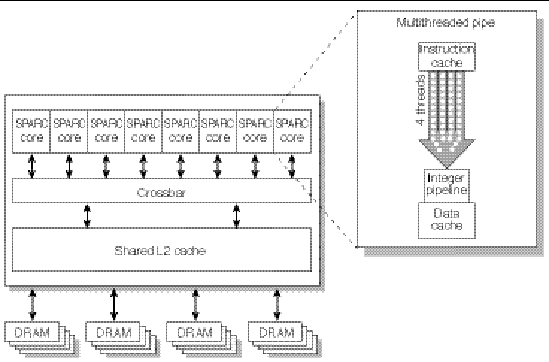
FIGURE 5-2 UltraSPARC T1 Multicore Processor Block Diagram
Each of the 8 SPARC cores has support for 4 threads, for a total of 32 threads. This support consists of a full register file per thread, with most ASI, ASR, and privileged registers replicated per thread. The 4 threads share the instruction cache, data cache, and TLBs. Each TLB is 64 entry.
Each core then has 16 Kbytes of primary Instruction Cache (I-cache) and 8 Kbytes of primary Data Cache (D-cache), each of which is parity protected with redundant rows and columns for repair.
Lastly there is 3-Mbyte unified L2 cache which is 12-way associative, ECC protected along with redundant rows and columns. This cache is shared among the 8 internal cores and is connected through an internal crossbar. The UltraSPARC T1 processor provides no external cache interface.
The UltraSPARC T1 processor contains four independent DDR-2 memory controllers and data interfaces. Unlike standard DDR-2 memory interfaces in the PC industry, the UltraSPARC T1 processor uses a 144-bit datapath to main memory. Thus, the DIMMs in a UltraSPARC T1 processor memory subsystem are always accessed two at a time. Because each DIMM provides 64 bits of data (plus ECC), the resulting data width is 128 bits (plus ECC).
The clock speed of the memory subsystem is nominally 200 MHz, which yields a data bit rate of 400 Mbps using the dual data rate signaling inherent to DDR-2 SDRAM technology.
The UltraSPARC T1 processor implements the standard SPARC V9 instruction set, along with the standard UltraSPARC III extensions, including the VIS instruction set, Interval Arithmetic support, and a special Prefetch Enhancement.
The UltraSPARC T1 processor follows the interrupt dispatch mechanisms laid down in the SunV architecture. In this model, interrupts are pushed into the CPU as Mondo Vectors which in UltraSPARC T1 systems take the form of Interrupt packets sent over the JBus interconnect from the JBus-to-PCI-E bridge into UltraSPARC T1 processor.
For reliability, availability, and serviceability (RAS), the UltraSPARC T1 processor provides parity protection on its internal cache memories, including tag parity and data parity on the D-cache and I-cache. The internal 3-Mbyte L2 cache has parity protection on the tags, and ECC protection on the data. The memory interface provides a standard Single-bit correct, Double-bit Detect ECC protection across the 128-bits of data, for a total memory width of 144 bits. In addition, the JBus interconnect is parity protected.
The UltraSPARC T1 processor supports a core frequency of 1 GHz. The maximum supported JBus speed is 200 MHz and maximum supported DDR-2 speed is 200 MHz.
The processor’s core speed, JBus, and DDR-2 speeds in the Sun Netra CP3060 blade server depend upon total blade server power budget, which shall not exceed 200W as per the PICMG 3.0 R1.0 specification.
The Sun Netra CP3060 blade server uses industry-standard DDR-2 VLP (0.72-inch) DIMMs. Each of the four memory controller units (MCUs) inside the UltraSPARC T1 processor can control up to four DIMMs. The Sun Netra CP3060 blade server only supports two DIMMs per MCU. The Sun Netra CP3060 blade server supports up to 2-Gbyte VLP DIMMs, for a total system memory capacity of 16 Gbytes.
Some of the key features of the memory subsystem are:
The organization of the memory subsystem with regard to the connections between the UltraSPARC T1 processor and the memory DIMMs is shown in FIGURE 5-3. Because the UltraSPARC T1 processor accesses memory with a 128-bit data path (plus ECC), DIMMs must be installed in pairs. The DIMMs are standard DDR-2 Registered VLP DIMMs. Specific vendors’ DIMMs are qualified by Sun and supplied as orderable options for system configuration.
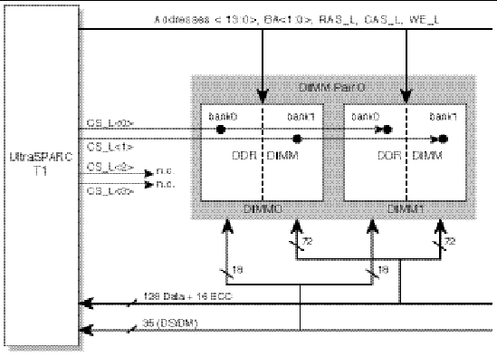
The ECC scheme employed by the UltraSPARC T1 memory controller provides single-bit correct, double-bit detect ECC protection across the 128 bits of data in each bank of memory. Also, each DIMM provides an industry-standard 256-byte Serial Presence Detect (SPD) PROM, of which 128 bytes are available to the system for dynamic FRU data. Plans are being made to use this 128 bytes for dynamic FRU data, such as soft error rate information.
The Sun Netra CP3060 blade server also supports the Chip-kill detect ECC scheme, allowing the detection of up to 4 bits in error, as long as they are not in the same DRAM. This is made possible by limiting the type of DDR-2 memory DIMMs to only include x4 organization.
The Sun Netra CP3060 blade server supports autoconfiguration using serial presence detect (SPD). The DIMMs have small EEPROM devices that store their configuration data according to the SPD format. MPC/vBSC reads this data via the I2C management bus, and writes the data into the OpenBoot PROM.
A 128-byte region of the SPD EEPROM is available for user data storage, allowing a limited form of FRU information to be implemented for the DIMMs.
The JBus is the main interconnect for the core of every UltraSPARC T1-based system. The JBus is a memory-coherent interconnect joining the UltraSPARC T1 processor to the JBus-to-PCI-E bridge.
JBus provides a memory-coherent 128-bit shared address/data path between each of the JBus resident devices. The JBus uses the Dynamic Termination Logic (DTL) signaling environment created initially for the UltraSPARC III, and is a globally clocked bus designed to run with a maximum clock frequency of 200 MHz. Memory coherence is maintained through the use of a snooping Modified-Owned-Exclusive-Invalid (MOESI) cache protocol, wherein all JBus agents must snoop their own cache hierarchies on every transaction that goes across the JBus interconnect.
JBus provides parity protection on all address and data transfers. One set of parity signals provides parity protection over the multiplexed address/data bus, and another provides parity over the control signals. Address and control parity errors cause a fatal reset, while data parity errors are treated on a per-instance basis, depending on the producer and consumer of the data.
The I/O subsystem implements the JBus and PCI-E fabrics, including the JBus-to-PCI-E bridge, one PCI-E switch, one AMC slot, two Intel PCI-E dual gigabit Ethernet chips, a PC-E UliM1575 Southbridge chip, and miscellaneous logic.
The JBus-to-PCI-E bridge is a low-cost, high-performance JBus-to-dual-PCI-E host bridge, similar to the PC-based Northbridge. On the host bus side, the JBus-to-PCI-E bridge supports a coherent, split-transaction, 128-bit JBus interface. On the I/O side, the JBus-to-PCI-E bridge supports two 8x-lane, industry-standard PCI-E interfaces. In addition, the JBus-to-PCI-E bridge supports the following interfaces/functionality to facilitate a richer system feature set.
The JBus unit detects which transactions present on JBus are targeted for the JBus-to-PCI-E bridge, accepts and queues those transactions, and coordinates with the appropriate destination unit within the JBus-to-PCI-E bridge to which the address and data are sent. When the UltraSPARC T1 processor is the target, the converse is true; in this case the JBus unit sends out onto the JBus the transactions initiated from within the JBus-to-PCI-E bridge (such as from one of the PCI units, I/O caches, and so on.), and presents them to the UltraSPARC T1 processor.
PCI-Express (PCI-E) is a high-speed, point-to-point dual simplex chip interconnect. It is designed as the next-generation system bus interconnect, replacing the aging PCI bus. PCI-E operates at 2.5 GHz and supports lane widths of x1, x2, x4, x8, x16, and x32.
PCI-E signaling is accomplished through the use of differential pairs per lane of the interface. For a 1x link, four individual lines are needed: TX+, TX-, RX+, and RX-. Electrically, the signaling levels are 1.2 volts.
PCI-E transfers data using packets. Each packet has a header which includes information about the packet and data payload. The data payloads vary in size from 64 bytes to 4 Kbytes. The maximum packet size supported for the JBus-to-PCI-E bridge is 512 bytes.
The Leaf A 4x PCI-E interface on the JBus-to-PCI-E bridge connects to the Extended Fabric NIC. The interface meets the PCI-E 1.0a specification and is completely autonomous from the second PCI-E interface on the JBus-to-PCI-E bridge. (That is, they are not electrically connected).
The Leaf B 8x PCI-E interface on the JBus-to-PCI-E bridge connects to the PCI-E Switch chip. The PLX chip then connects up to downsteam devices via 1x, 2x, 4x, or 8x links. (See PCI-E Switch for a better synopsis of the device).
The interface meets the PCI-E 1.0a specification and is completely autonomous from the first PCI-E interface on the JBus-to-PCI-E bridge. (that is, they are not electrically connected)
The JBus-to-PCI-E bridge employs a newly developed interrupt event queue that was necessitated by PCI-Express being able to generate many more interrupts (2M) than regular PCI, which was limited to four. The JBus-to-PCI-E chip supports 1-K coalesced interrupts.
The PCI-E switch supports full non-transparent crossbar bridging functionality that allows the system to isolate the I/O memory domains by presenting the processor subsystem as a endpoint rather than another memory system.
The eight ports on the PCI-E switch are highly configurable, allowing for lane widths from x1 up to x16. The Sun Netra CP3060 blade server only uses lane widths of x4 and x8, which are hard coded using strapping resistors on the port_config pins.
The signal strengths of SERDES outputs are controlled by software to better optimize power and signal levels. The four levels are off, low, typical, and high. The Sun Netra CP3060 blade server uses the typical setting.
The PCI-E switch provides a PC-Compliant Hot-Plug Controller per port. This is used at the port connected to the AMC modules.
This device is a PCI-E based gigabit Ethernet controller with two fully independent Media Access Control (MAC) and physical layer (PHY) ports. The PCI-E interface is fully compliant to the PCI Express Specification., Revision 1.0a.
The Sun Netra CP3060 blade server utilizes two controllers, one for the Base Fabric and one for the Extended Fabric.
Both Ethernet interfaces are compliant to the IEEE 802.3 standard for:
A serial SPI 16-KByte EEPROM is attached off each device to provide it with configuration data (PHY configuration data, MAC address, etc.).
The Sun Netra CP3060 blade server provides two gigabit Ethernet 10/100/1000BASE-T interfaces to meet the Base Interface requirements of ATCA. The Ethernet controller is used to provide dual Base Interfaces and is an integrated MAC and GMII. These controllers are connected to a x4 PCI-E link.
The controllers are coupled to the ATCA backplane for TPE network connection. Each interface supports 10BASE-T, 100BASE-TX, and 1000BASE-T operation, conforming to the IEEE802.3 specification (reference 11). The controllers individually negotiate transfer speeds when their network links are established.
The Sun Netra CP3060 blade server provides two gigabit Ethernet SERDES interfaces to meet the Extended Interface requirements of ATCA. This Ethernet controller is used to provide dual Extended Interfaces and includes a MAC and GMII. These controllers are connected to a x4 PCI-E link.
The Ethernet switch provides Base Interface connectivity to the MPC885.
The Sun Netra CP3060 blade server provides one AMC slot, Extended Full Height Single Width Card, used for PCI-E x8 expansion. In addition, a dual SATA channel from the Southbridge are wired to the AMC slot.
The SATA channels are wired to port 2 and port 3 on the AMC connector common options region (an AMC port is equal to a PCI-E lane; that is, two differential pairs).
Port 12-20 (8 differential signal pairs - total of 32 signals) on each AMC slot connector is wired to the Zone 3 RTM connector for AMC generated I/O.
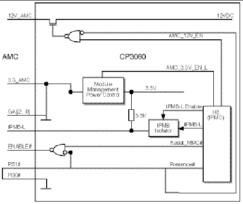
Power management is handled by the ATCA ShMC. An overview of the power and management signals is shown in FIGURE 5-4.
FIGURE 5-4 AMC Power and Management Infrastructure
See TABLE 5-1 for the IPMB-L addresses.
IPMC also provides individual reset (ENABLE# pin on the AMC connector) to the AMC slot by logically AND-ing the Reset_MMC# with the AMC PS1 input. Reset_MMC# is driven by the H8S GPIO pins.
The PS1# signal on the AMC connector provides presence indication. This signal is wired to an H8 GPIO pin.
When an AMC module is installed, the IPMC is signaled and will initially enable management power (3.3V) to the module. The IMPC will then have the ability to communicate with the module through the IPMI interface (IPMB_L). If the shelf manager controller (ShMC) determines that the module is supported, it signals the IPMC to enable payload power (12V) to the module. The IPMC controller will also assert HP_PRSNT# and HP_BUTTON# (ATTN#) inputs to the PCI-E switch hot-plug controller. This assertion will cause the switch to generate a hot-plug interrupt (or Presence detect change) to the processor to indicate that the blade server is hot inserted. This triggers a system event in the Solaris OS which causes an automatic connect/configure operation. When this operation completes, the processor asserts the HW_PWR_LED# output pin of the PCI-E switch hot-plug controller. This output is wired to the H8 GPIO pins.
An operator can initiate module removal by opening the module handle, which deactivates the hot-swap switch. When the hot-swap switch on the module is deactivated, the MMC in the module sends a module hot-swap (Module Handle Opened) event to the IPMC. If the ShMC permits blade server removal, the IPMC asserts the HP_BUTTON# input pin to the PCI-E switch hot-plug controller, which will generate a hot-plug event to the OS. When the OS has quiesced the driver operating the AMC module, the driver responds by writing to a CSR in the PCI-E switch that causes de-assertion of the HP_PWR_LED output pin. This signal is monitored by IPMC. When de-asserted, the IPMC informs the module to light the blue LED, then turns off payload power, and finally turns off management power.
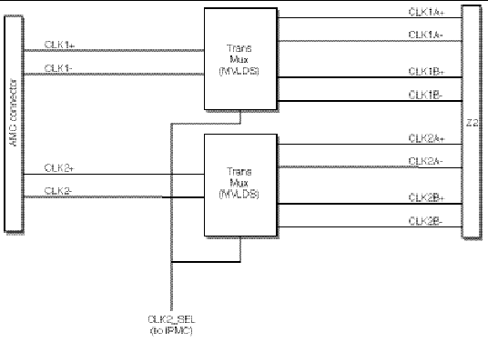
The Sun Netra CP3060 blade server routes the clock synchronization signals from the midplane (CLK1A/1B, CLK2A/2B) to the AMC slot connector CLK1 and CLK2 pins. The control of which clock signal (CLK1A or CLK1B and CLK2A or CLK2B) is routed to the corresponding CLK1 and CLK2 pins is handled by IPMC.
FIGURE 5-5 Clock Synchronization
The PCI-E-based Southbridge, when used in a PC system, implements virtually a complete desktop I/O subsystem, including Ethernet. Although many of the Super I/O functions built into the Southbridge are not used, functional blocks of the device are essential to the Sun Netra CP3060 blade server’s system architecture. Relative to the PCI-E interconnect, the Sun Netra CP3060 blade server uses a 4x link to access the M1575.
The major functional blocks used are listed below and described in the paragraphs which follow:
Configuring the internal devices of the Southbridge is very simple. There is a central switching/routing block inside the Southbridge chip that maps the PCI-E incoming data to the intended downstream device. Thus the Southbridge can be viewed as a collection of PCI devices within a single package. The functional units within Southbridge, which appear to firmware as unique PCI devices, are listed in TABLE 5-2. The Southbridge’s standard PCI device configuration is used to control the device behavior on the PCI bus and to allocate PCI Memory and I/O space address ranges needed by the device.
The IDE controller is resident inside the Southbridge. This is a dual controller but only the primary bus is utilized to connect the Compact Flash drive on the Sun Netra CP3060 blade server. The bus can operate at DMA mode 4 speed.
The Sun Netra CP3060 blade server provides the option of supporting an IDE Compact Flash card. In order to support higher memory capacity, a Type II CF socket is provided.
The Compact Flash card is not hot-swappable and there is no access to the CF socket once the blade server is installed in an ATCA chassis.
A dual 3-Gbps SATA port is connected to the AMC connector
The Sun Netra CP3060 blade server includes a MPC885 service processor subsystem used for LDOM configuration and Hypervisor interaction, host system reset, and boot support. The Sun Netra CP3060 blade server uses the MPC885 to run the vBSC firmware (on VxWorks). A block diagram of the subsystem is shown in FIGURE 5-1.
The following I/O interfaces provided by MPC885 are used by the Sun Netra CP3060 blade server:
There are three MPC external devices:
The SSI interface from the UltraSPARC T1 processor connects to a Field-Programmable Gate Array (FPGA) that provides an internal 32-Kbyte SRAM, access to external OpenBoot flash PROM through an XBus, and access to the IPMC and the MPC.
The FPGA serves as a gateway between the UltraSPARC T1 and the MPC subsystem and provides support functionality for the IPMC. It provides the following functionality:
The FPGA configuration is performed after an FPGA reset when the configuration is downloaded from the PROM. The PROM can be updated using a cable and the Xilinx programming header (JTAG), or from the MPC.
The 4-Mbyte flash PROM is used for the OpenBoot and POST firmware.
The Renesas H8S/2166 provides the IPM controller (IPMC) function on the Sun Netra CP3060 blade server. The IPMC provides PICMG 3.0 board management functionality, and it interfaces to the host CPU through a serial interface. The IPMC subsystem is powered from the standby power.
The IPMC is responsible for the following:
The BMR-H8S provides dual buffered Intelligent Platform Management Bus (IPMB) interfaces to the IPMB-0 bus on the PICMG 3.0 midplane. The I2C channels on the H8S are connected the IPMB-A and IPMB-B through the LTC4300A I2C buffers. The I2C buffers allow the board I2C to be isolated from the midplane until the board is fully seated and the I2C bus on the midplane is idle.
The BMR-H8S provides one serial payload interface to the MPC. This interface supports hardware flow control, RTS (Request To Send) and CTS (Clear To Send).
The H8S provides a local IPMI interface wired to the AMC slot (IPMB-L). The AMC IPMI interface is isolated through LTC4300A and controlled by H8 GPIO pins.
Hot-swap is supported by monitoring of the hot-swap handle switch. The handle switch goes directly to one of the GPIO pins on the H8S.
The hardware supports both non-graceful shutdown and graceful shutdown of payload in response to a hot-swap event. In case of non-graceful shutdown, firmware on the IPMC will disable the voltage rails before turning the blue LED on.
In case of graceful shutdown, IPMC writes to the SHUTDOWN_REQUEST bit in the FPGA, which will cause an interrupt to be sent to the JBus-to-PCI-E bridge and the MPC. When shutdown is complete, MPC signals this to IPMC through a status bit in the FPGA.
The Sun Netra CP3060 blade server supports three LEDs compliant with ATCA specification:
The LEDs are controlled by H8.
The BMR-H8S is able to control (enable/disable) power rails to the payload.
The BMR-H8S provides E-keying for the Extended interfaces to the midplane. PICMG mandates that the software hooks for E-keying be present, but it does not mandate that anything needs to be done in hardware in response to this. There is no hardware support for E-keying in the base interfaces. E-keying for the Extended interfaces is accomplished by setting the SIG_DET lines active.
FIGURE 5-6 is a block diagram of the I2C architecture. The subsequent subsections contain a description of the I2C Devices and Address map. The MPC has default access to the MPC_RUN_I2C bus..
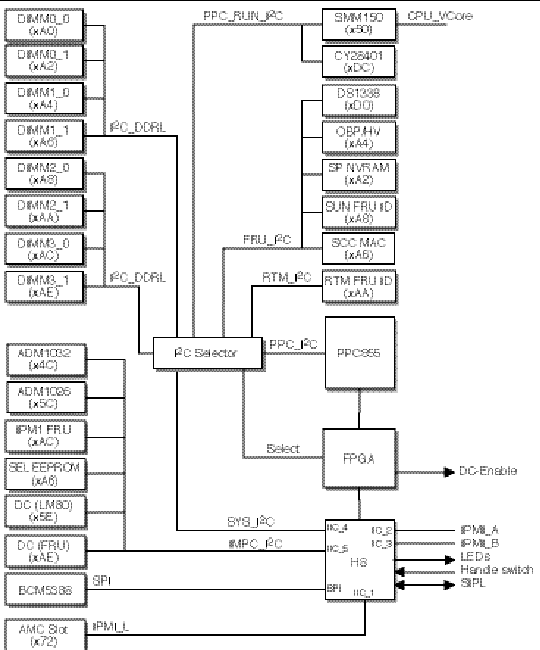
TABLE 5-3 shows the complete I2C address map for the I2C bus.
A few items are worth noting in the I2C address map shown above. The Address column indicates the I2C address for the associated device. Although the I2C address space is only 7 bits, the read/write bit is appended as bit <0>. Thus, the addresses listed here all represent the read form of the given device's address, that is, Addr<0>=0. These devices are solely accessed by the H8 on the motherboard (MB), if not otherwise noted in TABLE 5-3.
Note that a number of addresses are the same. This is possible because they are on different I2C segments controlled by the I2C MUX.
The Location column indicates the FRU on which the physical device resides. The Standby column indicates whether this device is readable when the system is in standby mode; that is, powered off but receiving its main power source. In other words, a YES in this column indicates that the H8 which is powered from the systems standby power rail, can access this device at all times, whether the system is powered on or off.
The system monitor (ADM1026) is a highly integrated and highly sophisticated multi-function system monitor, including Analog-to-Digital Conversion (ADC), Digital-to-Analog Conversion (DAC), Temperature Sensing, and GPIO pins.
The Analog Devices ADM1026 is used for system monitoring functions. The ADM1026 is interfaced with the IPMC, and the IPMC firmware is responsible for monitoring these sensors.
The ADM1026 measures most of the board voltages. The ADM1026 has one temperature sensor embedded in the device itself and supports two remote sensing channels requiring external diodes for temperature sensing. These remote sensors are used for measuring CPU die temperature.
The ADM1026 measures the voltages listed in TABLE 5-4. The ADM1206 and H8 firmware monitors these voltages. When the voltages are within regulations, the blade server functions with no warnings. When any voltage goes out of regulation beyond approximately ± 7percent, a Critical Warning is generated and presented to the shelf manager. When any voltage goes out of regulation beyond approximately ± 10%, the H8 initiates a blade server shutdown.
The ADM1026 also monitors the CPU die (or junction) temperatures of the CPU on the Sun Netra CP3060 blade server. The ADM1206 and H8 firmware reports a minor, major, or critical alarm when the temperature of either CPU goes beyond the thresholds listed in TABLE 5-5. Also, if the temperature of either CPU goes beyond the Emergency H8 Shutdown value listed in TABLE 5-5, the H8 initiates a blade server shutdown independent of the shelf manager.
The H8 temperature alarm equivalents are:
Minor Alarm = Upper Non Critical (UNC)
Major Alarm = Upper Critical (UC)
Critical Alarm = Upper Non Recoverable (UNR)
Emergency H8 Shutdown = Emergency H8 Shutdown (EMR)

|
Caution - These voltage and temperature thresholds should not be changed under normal operating conditions. |
The following list describes the power-on sequence:
1. Sun Netra CP3060 blade server installed into a midplane slot in ATCA shelf
2. Aux power applied to IPMC and the FPGA
3. IPMC enables front-end DC/DC (48V-12V converter)
4. IPMC checks power ok from front-end DC/DC
5. IPMC enables all voltage rails, and proceeds. if DC_OK
8. IPMC asserts SYSTEM_POK_ENABLE in FPGA CSRs.
9. SYSTEM_POK to JBus-to-PCI-E bridge F_PWR_GOOD is released (causes CPU hard reset), and vBSC commences with host reset sequence.
The following list provides an overview of the Sun Netra CP3060 blade server power rails:
The Sun Netra CP3060 blade server is powered from dual-redundant -48 V power supply inputs from the backplane power connector. It takes redundant -48V as input and derives the other necessary power using DC-DC converters. The design complies to the ATCA power distribution specification such as:
As required by the PICMG 3.0 R1.0 specification, the Sun Netra CP3060 blade server provides fuses on each of the -48V power feeds and on the return (RTN) connections. The fuses on the return feeds are critical to prevent overcurrent situations when an O-ring diode in the return path fails. There are eight fuses on the blade server connected to -48V_A, -48V_B, RET_A, RET_B, EARLY_A, EARLY_B, ENABLE_A, and ENABLE_B inputs. The fuses are one-time blow type fuse and need to be replaced when blown.
The Sun Netra CP3060 blade server uses the ATCA power module solution. The power module provides integrated ATCA power solution which supports PCIMG3.0 requirements including dual bus input, DC isolation, hold up, hot-plug, and management power (3.3V standby). It provides 12V intermediate bus as backend power. Some of the salient features of the module are:
The Sun Netra CP3060 blade server uses its own designed DC/DC SIP modules for generating other onboard power. All the voltages are generated from +12V input power.
The TOD clock battery must be type CR 1225, with a minimum of 4ma abnormal charging current rating (for example; a Panasonic CR 1225).

|
Caution - Risk of explosion if battery is replaced by an incorrect type.
Dispose of batteries properly in accordance with manufacturer’s instructions and local regulations. |
| Sun Netra CP3060 Blade Server User’s Guide | 819-4967-11 |
Copyright © 2009 Sun Microsystems, Inc. All rights reserved.