Use this appendix to reconfigure jumpers on the system and expansion memory boards, and when you add SIMM memory or identify a failing SIMM.
A jumper is a small metal sleeve that slides over two neighboring pins in a 3- pin header to provide an electrical connection. Pin 1 is identified by the square solder pad. See Figure A-1 and Figure A-2 to locate jumpers on both boards.
Table A-1 System Board Jumper Configuration
---------------------------------------------------------------------------------------------------


Label     Jumper  Default Configuration  Function
---------------------------------------------------------------------------------------------------
ARB1      J1701   1-2 IN                 Enable internal VME arbiter

ARB2      J1702   1-2 IN                 Enable internal VME arbiter

ARB4      J1703   1-2 IN                 Enable internal VME arbiter

ARB3      J1704   1-2 IN                 Enable internal VME arbiter

ARBDIS    J1705   1-2 OUT                Disable internal VME arbiter

VMERST    J1706   1-2 OUT                VME reset in

                  2-3 IN                 VME reset out

VME17     J1801   1-2 IN                 Enable VME IRQ7 to system board

VME 16            3-4 IN                 Enable VME IRQ6 to system board

VME15             5-6 IN                 Enable VME IRQ5 to system board

VME14             7-8 IN                 Enable VME IRQ4 to system board

VME13             9-10 IN                Enable VME IRQ3 to system board

VME12             11-12 IN               Enable VME IRQ2 to system board

VME11             13-14 IN               Enable VME IRQ1 to system board

None              15-16 OUT              Not used

VMCK      J1802   1-2 IN                 Enable VME 16 MHz clock (remove for in-circuit test)

SLOT1     J1803   1-2 IN                 Enable VME slot 1 functionality

SCSCK     J2202   1-2 IN                 Enable ESP-236 25 MHz clock

TDMSE     J2602   1-2 IN                 Disable TD mouse signal; read only

                  2-3 IN                 TD mouse controlled by 85C30; read/write (special function)

SERCK     J2603   1-2 IN                 Enable UART 19.6608 MHz clock (remove for in-circuit test)

232/423-  J2803   1-2 IN                 With J2804, sets serial ports to RS-223

                  2-3 IN                 With J2804, sets serial ports to RS-423A

232/423+  J2804   1-2 IN                 With J2803, sets serial ports to RS-232

                  2-3 IN                 With J2803, sets serial ports to RS-423A

FUNC-     J3201   1-2 IN                 Enable 80 MHz clock (remove for in-circuit test)

---------------------------------------------------------------------------------------------------

Table A-2 provides the jumper configurations for the expansion memory board.
------------------------------------------------------------------------------


Label               Jumper  Configuration  Function
------------------------------------------------------------------------------
Bank 0 installed    P3601   1-2            SIMMs installed in Bank 0
In, Out                     2-3            SIMMs not installed in Bank 0

Bank 1 installed    P3602   1-2            SIMMs installed in Bank 1
In, Out                     2-3            SIMMs not installed in Bank 1

Bank 2 installed    P3603   1-2            SIMMs installed in Bank 2
In, Out                     2-3            SIMMs not installed in Bank 2

Bank 3 installed    P3604   1-2            SIMMs installed in Bank 3
In, Out                     2-3            SIMMs not installed in Bank 3

Bank 0, 1 SIMMs     P3605   1-2            Double-sided SIMMs in Banks 0 and 1
Dbl, Sgl                    2-3            Single-sided SIMMS in Banks 0 and 1

Bank 2, 3 SIMMs     P360    1-2            Double-sided SIMMs in Banks 2 and 3
Dbl, Sgl                    2-3            Single-sided SIMMs in Banks 2 and 3

Board               P3607   1-2            Select memory board 2
1, 2                        2-3            Select memory board 1

Bank 3              P3301   1-2            80ns SIMMs installed
80ns, 100ns                 2-3            100ns SIMMs installed

Bank 2              P3302   1-2            80ns SIMMs installed
80ns, 100ns                 2-3            100ns SIMMs installed

Bank 1              P3303   1-2            80ns SIMMs installed
80ns, 100ns                 2-3            100ns SIMMs installed

Bank 0              P3304   1-2            80ns SIMMs installed
80ns, 100ns                 2-3            100ns SIMMs installed

------------------------------------------------------------------------------

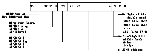
When a SIMM fails during Power-on Self-test (POST), the U-number, physical address, and board identification (memory- or system board) displays on the tty terminal.
Table A-3 Displayed Hex Value for Board/Bank
----------------------------------------------------------------------------------------------------


Displayed Hex Value                                                                   Board     Bank
----------------------------------------------------------------------------------------------------
0 x x x x x x x*                                                                      System    0

1 x x x x x x x                                                                       System    1

2 x x x x x x x  -  illegal  -  no Bank 2 on the system board

3 x x x x x x x  -  illegal  -  no Bank 3 on the system board

4 x x x x x x x                                                                       1st EXPM  0

5 x x x x x x x                                                                       1st EXPM  1

6 x x x x x x x                                                                       1st EXPM  2

7 x x x x x x x                                                                       1st EXPM  3

8 x x x x x x x                                                                       2nd EXPM  0

9 x x x x x x x                                                                       2nd EXPM  1

A x x x x x x x                                                                       2nd EXPM  2

B x x x x x x x                                                                       2nd EXPM  3

----------------------------------------------------------------------------------------------------
The method used to identify the indicted SIMM is unique to the particular operating system running on your system. To determine the U-number of the failed SIMM, perform the appropriate procedure below:
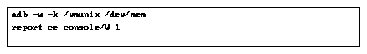
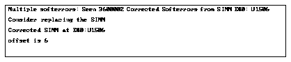
AFAR1, AFAR0 and AFSR should print out when the next error occurs.
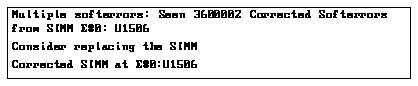
Figure A-3 Example Printout of Error Information
Note -
The important values presented in Figure A-3 are:
AFSR = 0x3401
AFAR0 = 0x9fc60d30
AFAR1 = 0x518fb8a0
Following steps below, use this information to determine the involved system
board or memory board, and to identify the u-number of the failed SIMM.

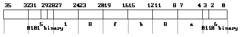
This is the block number.
From our example in Figure A-3, the AFSR value is used to produce the block number as follows:

So, AFSR [7:4] is 0; the block number is 0.

Determine the temporary offset as follows:
If the value of 11:8 is 4 or 5 (decimal), multiply the block number (noted
in step a) by 8 (see illustration below).

This yields the temporary offset value (in this example, "0").
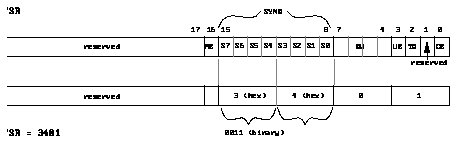
Using these eight bits
S7, S6, S5, S4 = 0011
S3, S2, S1, S0 = 0100
refer to Table A-4 to determine the syndrome code.
Table A-4 Syndrome Field Interpretation
---------------------------------------------------------------------------------------------


       S7                                    0   0   0   0   0   0   0   0   1   1   1   1   1   1   1   1
       S6                                    0   0   0   0   1   1   1   1   0   0   0   0   1   1   1   1
Syndrome   S5                                0   0   1   1   0   0   1   1   0   0   1   1   0   0   1   1
  Bits     S4                                0   1   0   1   0   1   0   1   0   1   0   1   0   1   0   1

S3 S2   S1 S0
---------------------------------------------------------------------------------------------
0  0  0  0                                   *   C4  C5  D   C6  D   D   T   C7  D   D   T   D   T   T   Q

0  0  0  1                                   C0  D   D   00  D   25  M   D   D   05  17  D   08  D   D   12

0  0  1  0                                   C1  D   D   01  D   29  36  D   D   M   21  D   13  D   D   09

0  0  1  1                                   D   32  33  D   42  D   D   M   47  D   D   M   D   T   T   D

0  1  0  0                                   C2  D   D   10  D   27  07  D   D   M   19  D   02  D   D   14

0  1  0  1                                   D   57  61  D   59  Q   D   M   63  D   Q   M   D   M   M   D

0  1  1  0                                   D   M   04  D   39  D   D   22  M   D   D   30  D   16  24  D

0  1  1  1                                   T   D   D   M   D   M   54  D   D   50  M   D   T   D   D   M

1  0  0  0                                   C3  D   D   15  D   31  M   D   D   38  23  D   03  D   D   11

1  0  0  1                                   D   37  M   D   M   D   D   18  06  D   D   26  D   20  28  D

1  0  1  0                                   D   49  53  D   51  Q   D   M   55  D   Q   M   D   M   M   D

1  0  1  1                                   T   D   D   M   D   M   62  D   D   58  M   D   T   D   D   M

1  1  0  0                                   D   40  45  D   34  D   D   T   35  D   D   T   D   M   M   D

1  1  0  1                                   T   D   D   T   D   M   48  D   D   52  M   D   M   D   D   M

1  1  1  0                                   T   D   D   T   D   M   56  D   D   60  M   D   M   D   D   M

1  1  1  1                                   Q   44  41  D   46  D   D   M   43  D   D   M   D   M   M   Q

*     No error detected

D     	Double-bit error

T     Triple-bit error

Q     Quadruple-bit error

M     More than 4-bit error

Numeric Bit number os the single-bit error

---------------------------------------------------------------------------------------------
Note that in our example
S7, S6, S5, S4 = 0011
S3, S2, S1, S0 = 0100
the syndrome code is 10:
--------------------------------------------------------------------


       S7           0   0   0   0   0   0   0   0   1   1   1   1   1   1   1   1
       S6           0   0   0   0   1   1   1   1   0   0   0   0   1   1   1   1
Syndrome   S5       0   0   1   1   0   0   1   1   0   0   1   1   0   0   1   1
  Bits     S4       0   1   0   1   0   1   0   1   0   1   0   1   0   1   0   1

S3 S2   S1 S0
--------------------------------------------------------------------
0  0  0  0          *   C4  C5  D   C6  D   D   T   C7  D   D   T   D   T   T   Q

0  0  0  1          C0  D   D   00  D   25  M   D   D   05  17  D   08  D   D   12

0  0  1  0          C1  D   D   01  D   29  36  D   D   M   21  D   13  D   D   09

0  0  1  1          D   32  33  D   42  D   D   M   47  D   D   M   D   T   T   D

0  1  0  0          C2  D   D   10  D   27  07  D   D   M   19  D   02  D   D   14

0  1  0  1          D   57  61  D   59  Q   D   M   63  D   Q   M   D   M   M   D

--------------------------------------------------------------------
Table A-5 Method Used to Identify the Faulty SIMM
------------------------------------------------------------------------------------------------------------------------------------------


Syndrome Code Value  Nature of Failure    Diagnosis                 Offset Computation Method
------------------------------------------------------------------------------------------------------------------------------------------
0 Through 63         Single byte error    Identify the faulty SIMM  offset = offset1 and (7-syn_code/8).
                                                                    Use AFAR1 and 0x0xfffffff8 + offset as the
                                                                    physical address for decoding.

64 Through 71        Single byte error    Identify the faulty SIMM  offset = offset and (7-syn_code mod 8).
                                                                    Use AFAR1 and 0x0xfffffff8 + offset as the
                                                                    physical address for decoding.

72 or Greater        Multiple byte error  Identify the group of 8   The 8 true physical addresses are:
                                          SIMMs which is failing
                                                                    AFAR1 and 0xfffffff8 + 0
                                                                    AFAR1 and 0xfffffff8 + 1
                                                                    AFAR1 and 0xfffffff8 + 2
                                                                    AFAR1 and 0xfffffff8 + 3
                                                                    AFAR1 and 0xfffffff8 + 4
                                                                    AFAR1 and 0xfffffff8 + 5
                                                                    AFAR1 and 0xfffffff8 + 6
                                                                    AFAR1 and 0xfffffff8 + 7

------------------------------------------------------------------------------------------------------------------------------------------
Given that the syndrome code established in step c above is 10, the row "0 through 63" in Table A-5 applies since 10 is within the range 0-63.
--------------------------------------------------------------------------------------------------------------


Syndrome Code Value  Nature of Failure  Diagnosis                 Offset Computation Method
--------------------------------------------------------------------------------------------------------------
0 Through 63         Single byte error  Identify the faulty SIMM  offset = offset1 and (7-syn_code/8).
                                                                  Use AFAR1 and 0x0xfffffff8 + offset as the
                                                                  physical address for decoding.

--------------------------------------------------------------------------------------------------------------
Offset = offset + (7 -10/8)
Our offset is 0
Offset = 0 + (7 -10/8)
= 0 + (7 -1)
= 6
(AFAR1 and 0xfffffff8) + offset
= 0x518fb8a0 and 0xfffffff8 + 6
= 0x 0x518fb8a0 + 6
= 0x518fb8a6
From the example above, bits [31:28] are 5.
-----------------------------------------------------------------------


PA       PA [2:0]: 000   001     010     011     100     101     110    111
29,28,3  Data:	63:56 55:48   47:40   39:32   31:24   23:16   15:8   7:0
         ECC:	7      6       5       4       3       2       1      0
-----------------------------------------------------------------------
0 0 0    U1805           U1801   U1705   U1701   U1605   U1601   U1505  U1501

0 0 1    U1807           U1803   U1707   U1703   U1607   U1603   U1507  U1503

0 1 0    U1806           U1802   U1706   U1702   U1606   U1602   U1506  U1502

0 1 1    U1808           U1804   U1708   U1704   U1608   U1604   U1508  U1504

-----------------------------------------------------------------------
The failing SIMM is on the 1st expansion memory board in location U1506.

An ECC correctable error is reported only when there are more that 256 errors for each SIMM. By default, this prints only to the log file. Override default reporting using the procedure below.
AFAR1, AFAR0 and AFSR should print out when the next error occurs.
o SIMM number
o Offset of the error byte in the 8/16/32 byte transaction
o Bits in error
o Physical addresses of the start of the 8/16/32 byte group in error
An example appears below:
In this case,
(0x518fb8a0 AND fffffff8) + 6
The following tables and figure are supplemental information.
Table A-6 SIMM U-Numbers for System Board
-----------------------------------------------------------------------


PA 28,3  PA [2:0]: 000   001     010     011     100     101     110    111
         Data:	63:56 55:48   47:40   39:32   31:24   23:16   15:8   7:0
         ECC:	7      6       5       4       3       2       1      0
-----------------------------------------------------------------------
0 0      U1201           U1203   U1205   U1207   U1101   U1103   U1105  U1107

0 1      U1401           U1403   U1405   U1407   U1301   U1303   U1305  U1307

1 0      U1202           U1204   U1206   U1208   U1102   U1104   U1106  U1108

1 1      U1402           U1404   U1406   U1408   U1302   U1304   U1306  U1308

-----------------------------------------------------------------------
Table A-7 SIMM U-Numbers for Memory Board
-----------------------------------------------------------------------


PA       PA [2:0]: 000   001     010     011     100     101     110    111
29,28,3  Data:	63:56 55:48   47:40   39:32   31:24   23:16   15:8   7:0
         ECC:	7      6       5       4       3       2       1      0
-----------------------------------------------------------------------
0 0 0    U1805           U1801   U1705   U1701   U1605   U1601   U1505  U1501

0 0 1    U1807           U1803   U1707   U1703   U1607   U1603   U1507  U1503

0 1 0    U1806           U1802   U1706   U1702   U1606   U1602   U1506  U1502

0 1 1    U1808           U1804   U1708   U1704   U1608   U1604   U1508  U1504

1 0 0    U2205           U2201   U2105   U2101   U2005   U2001   U1905  U1901

1 0 1    U2207           U2203   U2107   U2103   U2007   U2003   U1907  U1904

1 1 0    U2206           U2202   U2106   U2102   U2006   U2002   U1906  U1902

1 1 1    U2208           U2204   U2108   U2104   U2008   U2004   U1908  U1904

-----------------------------------------------------------------------