
-----------------------------------------------------------------------


Connector Locations                                        page C-1

Parallel Connector                                         page C-2

Audio/AUI Connector                                        page C-3

AUI Connector                                              page C-4

Keyboard and Mouse Connector                               page C-5

ISDN Connectors                                            page C-5

Serial Ports A and B Connector                             page C-6

Twisted Pair Ethernet Connector                            page C-7

SCSI Connector                                             page C-7

13W3 Connector                                             page C-9

Audio Ports and Audio Module - S10BSX Service Code Systems page C-10

-----------------------------------------------------------------------
Chapter 1, "Product Description" shows the back panel of the system illustrating the connector locations.
The following sections describe each connector on the back panel. Table C-1 through Table C-12 show the pin assignments, signal descriptions, and an illustration of each connector.
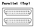
Table C-1 Parallel Connector Pin Assignments
-------------------------------------------------------------------


Pin                   Function     Signal Description  I/O  Level
-------------------------------------------------------------------
1                     DataStrobe*  Data valid Strobe   I/O  24 ma OC

2                     Data Bit 0   Data Bit 0          I/O  24 ma OC

3                     Data Bit 1   Data Bit 1          I/O  24 ma OC

4                     Data Bit 2   Data Bit 2          I/O  24 ma OC

5                     Data Bit 3   Data Bit 3          I/O  24 ma OC

6                     Data Bit 4   Data Bit 4          I/O  24 ma OC

7                     Data Bit 5   Data Bit 5          I/O  24 ma OC

8                     Data Bit 6   Data Bit 6          I/O  24 ma OC

9                     Data Bit 7   Data Bit 7          I/O  24 ma OC

10                    Ack*         Data Acknowledge    I    TTL

11                    Busy         Busy                I    TTL

12                    PE           Paper Error         I    TTL

13                    Select       Select              I    TTL

14                    AutoFeed*    AutoFeed            O    24 ma TTL

15                    Error*       Error               I    TTL

16                    Reset*       Initialize          O    24 ma TTL

17                    SlctIn*      Select In           O    24 ma TTL

18                    Shield                                GND

19                    Shield                                GND

20                    Shield                                GND

21                    Shield                                GND

22                    Shield                                GND

23                    Shield                                GND

24                    Shield                                GND

25                    Shield                                GND

26                    Shield                                GND

*  Active low signal

-------------------------------------------------------------------
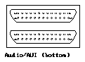
Table C-2 Audio/AUI Connector Pin Assignments
-----------------------------------------------------------


Pin  Function    I/O  Level   Signal Description
-----------------------------------------------------------
1    AUI_DO-     O    Analog  Data Out Positive/Negative

2    AUI_DI+     I    Analog  Data Out Positive/Negative

3    AUI_CI-     I    Analog  AUI Collision Positive/Negative

4    +12 VDC     O    DC

5    EMCTL       I&O   TTL     External Mode Control

6    CHI_DX      I&O   TTL     Digital Audio Data Transmit

7    CHI_CLK     I&O   TTL     Digital Audio Clock

8    CHI_DFSYNC  I&O   TTL     Digital Audio Frame Sync

9    N.C.

10   +5 VDC      O    DC

11   +5VDC       O    DC

12   ExtPwrDn    I    TTL

13   +5 VDC      O    DC

14   AUI_DO+     O    Analog  Data Out Positive/Negative

15   AUI_DI_     I    Analog  Data Out Positive/Negative

16   AUI_CI+     I    Analog  AUI Collision Positive/Negative

17   Ground           GND

18   CHI_ResetS  I&O   TTL     Digital Audio Reset

19   CHI_DR      I&O   TTL     Digital Audio Data Receive

20   CHI_FS      I&O   TTL

21   D/C         I&O   TTL     Data/Control Select

22   N.C.

23   Ground           GND

24   Ground      O    GND

25   N.C.

26   Ground           GND

-----------------------------------------------------------
The Audio/AUI connector is installed only on the S10 service code model.
The AUI connector is installed only on the SPARCstation 10 system with the S10BSX service code.
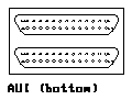
Table C-3 AUI Connector Pin Assignments
---------------------------------------------------------


Pin  Function  I/O  Level   Signal Description
---------------------------------------------------------
1    AUI_DO-   O    Analog  Data Out Positive/Negative

2    AUI_DI+   I    Analog  Data Out Positive/Negative

3    AUI_CI-   I    Analog  AUI Collision Positive/Negative

4    +12 VDC   O    DC

5    N.C .

6    N.C .

7    N.C .

8    N.C .

9    N.C .

10   N.C .

11   N.C .

12   N.C .

13   N.C .

14   AUI_DO+   O    Analog  Data Out Positive/Negative

15   AUI_DI_   I    Analog  Data Out Positive/Negative

16   AUI_CI+   I    Analog  AUI Collision Positive/Negative

17   Ground         GND

18   N.C .

19   N.C .

20   N.C .

21   N.C .

22   N.C.

23   N.C .

24   N.C .

25   N.C.

26   Ground         GND

---------------------------------------------------------

--------------------------------------------------------------


Pin                   Function   I/O  Level  Signal Description
--------------------------------------------------------------
1                     Ground     O    GND

2                     Ground     O    GND

3                     +5 VDC     O    VCC

4                     Mouse In   I    TTL    Input From Mouse

5                     KeyBd Out  O    TTL    Output to Keyboard

6                     KeyBd In   I    TTL    Input from Keyboard

7                     PowerOn*   I    TTL    Power on key

8                     +5VDC      O    VCC

*  Active low signal

--------------------------------------------------------------
ISDN connectors are on specific models of the S10 service code only.

Table C-5 ISDN Connectors Signal Descriptions
-------------------------------------------------------------


Signal       Description
-------------------------------------------------------------
OUT_NT3 +/-  Differential External Power Supply Source (NC)

NT_In +/-    Differential Network Terminator Data Input

NT_Out +/-   Differential Network Terminator Data Output

OUT_Nt@ +/-  Differential Internal Power Supply Source

OUT_TE3 +/-  Differential Internal Power Supply Source  (NC)

TE_OUT +/-   Differential Terminal Equipment Data Output

TE_In +/-    Differential Terminal Equipment Data Input

OUT_TE2 +/-  Differential External Power Supply Source

-------------------------------------------------------------
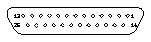
Table C-6 Serial Port A/B Pin Assignments
------------------------------------------------------------------


Pin    Function     I/O  Level      Signal Description
------------------------------------------------------------------
1      N.C.

2      Xmit Data A  O    RS232/423  Xmit Data A/Transmit Data Port A

3      Rec Data A   I    RS232/423  Receive Data Port A

4      RTS A        O    RS232/423  Request to Send Port A

5      CTS A        I    RS232/423  Clear to Send Port A

6      DSR A        I    RS232/423  Data Set Ready Port A

7      Ground            GND

8      DCD A        I/O  RS232/423  Data Carrier Detect Port A

9      N.C.

10     N.C.

11     DTR B        I    RS232/423  Data Terminal Ready Port B

12     DCD B        I    RS232/423  Data Carrier Detect Port B

13     CTS B        I    RS232/423  Clear To Send Port B

14     Xmit Data B  O    RS232/423  Transmit Data Port B

15     TRxC A       I    RS232/423  Receive/Transmit Clock Port A
                                    (Pullup)

16     Rec Data B   I    RS232/423  Receive Data Port B

17     RTxC A       I    RS232/423  Secondary/Transmit Clock
                                    (Receive) Port

18     TRxC B       I    RS232/423  Receive/Transmit Clock Port B
                                    (Pullup)

19     RTS B        O    RS232/423  Request to Send Port B

20     DTR A        O    RS232/423  Data Terminal Ready Port A

21-23  N.C.

24     TxC A        O    RS232/423  Transmit Clock Port A

25     TxC B        O    RS232/423  Transmit Clock Port B

------------------------------------------------------------------
Note - TRxC A and TxC A are connected to the same bidirectional pin.

Table C-7 Twisted Pair Ethernet Pin Assignments
------------------------------------------------------------


Pin  Function  I/O  Level   Signal Description
------------------------------------------------------------
1    TPO+      O    Analog  Differential Twisted Pair
                            Transmit Data

2    TPO-      O    Analog  Differential Twisted Pair
                            Transmit Data

3    TPI+      I    Analog  Differential Twisted Pair Receive
                            Data

4    N.C.

5    N.C.

6    TPI-      I    Analog  Differential Twisted Pair Receive
                            Data

7    N.C.

8    N.C.

------------------------------------------------------------
Table C-8 shows the pin assignments, signal description, and an illustration of the SCSI connector on the back panel of the system.
Table C-8 SCSI Pin Assignments
--------------------------------------------------------------------------------


Pin                  Function  Level  Pin  Function   I/O  Level  Description
--------------------------------------------------------------------------------
1                    Ground    GND    26   sd0*       I&O   TTL    SCSI Data Bit 0

2                    Ground    GND    27   sd1*       I&O   TTL    SCSI Data Bit1

3                    Ground    GND    28   sd2*       I&O   TTL    SCSI Data Bit 2

4                    Ground    GND    29   sd3*       I&O   TTL    SCSI Data Bit 3

5                    Ground    GND    30   sd4*       I&O   TTL    SCSI Data Bit 4

6                    Ground    GND    31   sd5*       I&O   TTL    SCSI Data Bit 5

7                    Ground    GND    32   sd6*       I&O   TTL    SCSI Data Bit 6

8                    Ground    GND    33   sd7*       I&O   TTL    SCSI Data Bit 7

9                    Ground    GND    34   sdp*       I&O   TTL    SCSI Data Parity

10                   Ground    GND    35   Ground          GND

11                   Ground    GND    36   Ground          GND

12                   Ground    GND    37   Ground          GND

13                   Ground    GND    38   Termpower  I&O   TTL    Termination Voltage

14                   Ground    GND    39   Ground          GND

15                   Ground    GND    40   Ground          GND

16                   Ground    GND    41   atn*       O    TTL    Attention

17                   Ground    GND    42   Ground          GND

18                   Ground    GND    43   bsy*       O    TTL    Busy

19                   Ground    GND    44   ack*       O    TTL    Acknowledge

20                   Ground    GND    45   rst*       O    TTL    Reset

21                   Ground    GND    46   msg*       O    TTL    Message

22                   Ground    GND    47   sel*       O    TTL    Select

23                   Ground    GND    48   cd*        O    TTL    Control/Data

24                   Ground    GND    49   req*       O    TTL    Request

25                   Ground    GND    50   io*        O    TTL    Input/Output

* Active low signal

--------------------------------------------------------------------------------
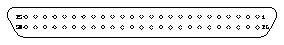
Table C-9 shows the pin assignments, function, and a picture of the 13W3 connector. This connector is built into the S10BSX service code (as noted on the system board). For the S10 service code, you must insert a video frame buffer card with a 13W3 connector on it into one of the SBus slots to drive the monitor.

Table C-9 13W3 Connector Pin Assignments
-----------------------------


Pin  Function      I/O  Level
-----------------------------
A1   Red           O    Analog

A2   Green         O    Analog

A3   Blue          O    Analog

1    Serial Read        TTL

2    Vert Sync     O    TTL

3    Sense <0'>     I    TTL

4    Ground             GND

5    Comp Sync     O    TTL

6    Hort Sync     O    TTL

7    Serial Write       TTL

8    Sense <1'>     I    TTL

9    Sense <2'>     I    TTL

10   Ground             GND

-----------------------------
The audio ports are on the model with the S10BSX service code on the system board. Table C-10 gives the signals for the audio ports.
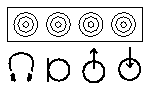
Table C-10 Signals for the Audio Ports
-----------------------------------------------------------------------------------


               Headphone      Microphone   Microphone     Line-Out       Line-In
                                           (new)
                              (old)
-----------------------------------------------------------------------------------
Tip            Left Channel   Mono In      Left Channel   Left Channel   Left Channel

Ring (Center)  Right Channel  Microphone   Right Channel  Right Channel  Right Channel
                              power


Shield         Return         Ground       Return         Return         Return

-----------------------------------------------------------------------------------
This connector is for connecting a set of stereophonic headphones to the system for private listening of audio output.

This connector is used to connect the Sun Microphone to the system to provide it with voice input.

This connector is to connect the system audio output to a stereophonic amplifier and external loudspeakers.

This connector is to connect external sound sources such as a compact disc player or cassette tape player to the system.

The audio module has two connectors, a digital connector and an audio connector. Table C-11 and Table C-12 list the signals for the two audio module connectors.
Table C-11 Pinout of Audio Module Digital Connector
----------------------------------------------


Pin  Signal               Pin  Signal
----------------------------------------------
1    Speaker Negative     16   Speaker Positive

2    Ground               17   Ground

3    Active low           18   NC

4    SBI Reset            19   SBI Alternate
                               Power Down

5    NC                   20   +12V

6    SBI Used Power Down  21   +12V

7    SBI Data/Control     22   +12V

8    +5V                  23   +5V

9    NC                   24   +5V

10   SBI Time Slot Out    25   +5V

11   Ground               26   Ground

12   Ground               27   Ground

13   SBI Frame Sync       28   Ground

14   SBI Data Transmit    29   SBI Time Slot In

15   SBI Clock            30   SBI Data Receive

----------------------------------------------
Table C-12 Pinout of Audio Module Analog Connector
---------------------------------------------------


Pin  Signal                   Pin  Signal
---------------------------------------------------
1    Headphone Ring (Center)  16   Headphone Tip

2    Headphone Shield         17   Headphone Shield

3    Chassis Ground           18   Chassis Ground

4    Chassis Ground           19   Chassis Ground

5    Microphone Tip           20   Microphone Ring
                                   (Center)

6    Microphone Shield        21   Microphone Shield

7    Chassis Ground           22   Chassis Ground

8    Chassis Ground           23   Chassis Ground

9    Line Out Ring (Center)   24   Line Out Tip

10   Line Out Shield          25   Line Out Shield

11   Chassis Ground           26   Chassis Ground

12   Chassis Ground           27   Chassis Ground

13   Line In Tip              28   Line In Ring
                                   (Center)

14   Line In Shield           29   Line In Shield

15   Chassis Ground           30   Chassis Ground

---------------------------------------------------
