A P P E N D I X  B

Connectors, Pinouts, and Switch Settings

This chapter contains the following sections:


Note - For pin assignments of the rear transition module connectors, refer to the Netra CP2500 Rear Transition Module Installation and Technical Reference Manual (819-1753).


B.1 PMC Connector

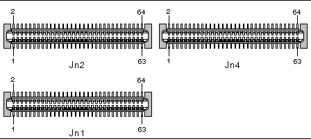
FIGURE B-1 and FIGURE B-2 show the location of PMC port connectors and pins. The following tables define contact allocations.


FIGURE B-1 Netra CP2500 Board PMC Port Connectors

Figure showing the location of the PMC slot and PMC connectors.


Note - The P1386.1 standard reserves the Jn3 64-pin connector for PCI 64-bit extensions, so it is not fitted on the Netra CP2500 board.


FIGURE B-2 PMC Connector Slot Connector Pins

Figure showing the PMC slot connector pin numbering.


B.1.1 PMC Connector Interfaces

Corresponding to the Common Mezzanine Card (CMC) specification, the PMC A slot is comprised of three PMC connectors - Jn1, Jn2, and Jn4. (The Jn3 connector is not fitted on the Netra CP2500 board.)


Note - Sun does not support installing a PIM device on either the RTM-S or the RTM-H.


The following tables list the PMC slot connector interfaces.


TABLE B-1 PMC Jn1 Connector Interface

Pin

Description

Pin

Description

1

Not connected

2

-12V

3

GND

4

PMC_A_INT_A_L

5

PMC_A_INT_B_L

6

PMC_A_INT_C_L

7

PMC_BUSMODE1_L[1]

8

VCC (5V)

9

PMC_A_INT_D_L

10

NC

11

GND

12

NC

13

PMC_CLK

14

GND

15

GND

16

PMC_GNT_L

17

PMC_REQ_L

18

VCC

19

LOCAL_VIO

20

PCI_B_AD<31>

21

PCI_B_AD<28>

22

PCI_B_AD<27>

23

PCI_B_AD<25>

24

GND

25

GND

26

PCI_B_CBE3_L

27

PCI_B_AD<22>

28

PCI_B_AD<21>

29

PCI_B_AD<19>

30

VCC

31

LOCAL_VIO

32

PCI_B_AD<17>

33

PCI_B_FRAME_L

34

GND

35

GND

36

PCI_B_IRDY_L

37

PCI_B_DEVSEL_L

38

VCC

39

GND

40

PCI_B_LOCK_L

41

PMC_SDONE

42

PMC_SB0_L

43

PCI_B_PAR

44

GND

45

LOCAL_VIO

46

PCI_B_AD<15>

47

PCI_B_AD<12>

48

PCI_B_AD<11>

49

PCI_B_AD<9>

50

VCC

51

GND

52

PCI_B_CBE_L<0>

53

PCI_B_AD<6>

54

PCI_B_AD<5>

55

PCI_B_AD<4>

56

GND

57

LOCAL_VIO

58

PCI_B_AD<3>

59

PCI_B_AD<2>

60

PCI_B_AD<1>

61

PCI_B_AD<0>

62

VCC

63

GND

64

PCI_B_REQ64_L


TABLE B-2 PMC Jn2 Connector Interface

Pin

Description

Pin

Description

1

+12V

2

JTAG_PMC_RST_L

3

TMS

4

PMC_TDO

5

PMC_TDI

6

GND

7

GND

8

NC

9

NC

10

NC

11

PMC_BUSMODE2_L

12

VDD (3.3V)

13

PCI_B_RST_L

14

PMC_BUSMODE3_L

15

VDD

16

PMC_BUSMODE4_L

17

NC

18

GND

19

PCI_B_AD<30>

20

PCI_B_AD<29>

21

GND

22

PCI_B_AD<26>

23

PCI_B_AD<24>

24

VDD

25

PCI_B_IDSEL

26

PCI_B_AD<23>

27

VDD

28

PCI_B_AD<20>

29

PCI_B_AD<18>

30

GND

31

PCI_B_AD<16>

32

PCI_B_CBE_L<2>

33

GND

34

NC

35

PCI_B_TRDY_L

36

VDD

37

GND

38

PCI_B_STOP_L

39

PCI_B_PERR_L

40

GND

41

VDD

42

PCI_B_SERR_L

43

PCI_B_CBE_L<1>

44

GND

45

PCI_B_AD<14>

46

PCI_B_AD<13>

47

GND

48

PCI_B_AD<10>

49

PCI_B_AD<8>

50

VDD

51

PCI_B_AD<7>

52

NC

53

VDD

54

NC

55

NC

56

GND

57

NC

58

NC

59

GND

60

NC

61

PCI_B_ACK64_L

62

VDD

63

GND

64

NC


Note - The P1386.1 standard reserves the Jn3 64-pin connector for PCI 64-bit extensions. It is not fitted on these boards.


TABLE B-3 PMC Jn4 Connector Interface

Pin

Description

Pin

Description

1

Not connected

2

Not connected

3

Not connected

4

Not connected

5

Not connected

6

Not connected

7

Not connected

8

Not connected

9

Not connected

10

Not connected

11

Not connected

12

Not connected

13

Not connected

14

Not connected

15

Not connected

16

Not connected

17

Not connected

18

Not connected

19

Not connected

20

Not connected

21

Not connected

22

Not connected

23

Not connected

24

Not connected

25

Not connected

26

Not connected

27

Not connected

28

Not connected

29

Not connected

30

Not connected

31

Not connected

32

Not connected

33

PMC_A_IO_33

34

PMC_A_IO_34

35

PMC_A_IO_35

36

PMC_A_IO_36

37

PMC_A_IO_37

38

PMC_A_IO_38

39

PMC_A_IO_39

40

PMC_A_IO_40

41

PMC_A_IO_41

42

PMC_A_IO_42

43

PMC_A_IO_43

44

PMC_A_IO_44

45

PMC_A_IO_45

46

PMC_A_IO_46

47

PMC_A_IO_47

48

PMC_A_IO_48

49

Not connected

50

Not connected

51

Not connected

52

Not connected

53

Not connected

54

Not connected

55

Not connected

56

Not connected

57

Not connected

58

Not connected

59

Not connected

60

Not connected

61

Not connected

62

Not connected

63

Not connected

64

Not connected


B.2 Front Panel Serial Connector

This section contains the pin assignments for the front panel serial port connector.
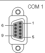

FIGURE B-3 Front Panel Serial Port Diagram

Figure showing the pin diagram of the front panel serial port.


TABLE B-4 shows the serial port connector (TTYA) pin assignments.


TABLE B-4 Serial Micro DB9 Connector Pinouts

Pin

Signal Name

Pin

Signal Name

1

SER_DCD

6

SER_OSR

2

SER_RXD

7

SER_RTS

3

SER_TXD

8

SER_CTS

4

SER_DTR

9

SER_RI

5

SER_GND


B.3 Backplane Connectors

FIGURE B-4 shows contact numbering as seen from the back of the Netra CP2500 board.
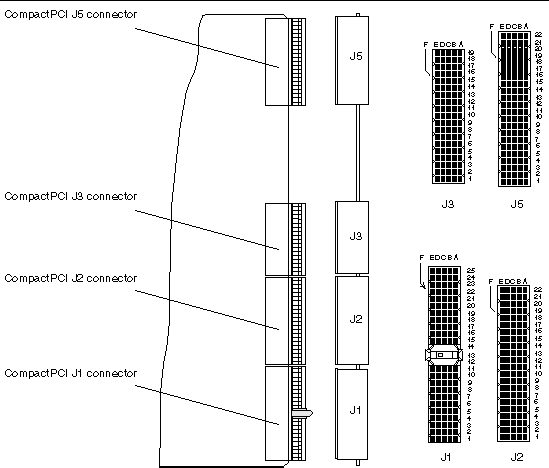

FIGURE B-4 Backplane Connector Contact Numbering

Figure showing the location and labelling of the backplane connectors.


Note - The CompactPCI J4 connector is not populated on the Netra CP2500 board.


B.3.1 CompactPCI J1/P1 Connector Pinouts

TABLE B-5 lists the CompactPCI J1/P1 connector pin assignments.


TABLE B-5 CompactPCI J2/P2 Connector Pin Assignments

Pin

Row Z

Row A

Row B

Row C

Row D

Row E

Row F

25

GND

+EP_5V

CPCI_REQ64#

CPCI_ENUM#

+EP_3.3V

+EP_5V

GND

24

GND

CPCI_AD[1]

+EP_5V

LP_VIO/unused

CPCI_AD[0]

CPCI_ACK64#

GND

23

GND

+EP_3.3V

CPCI_AD[4]

CPCI_AD[3]

LP_+EP_5V

CPCI_AD[2]

GND

22

GND

CPCI_AD[7]

GND

LP_+EP_3.3V

CPCI_AD[6]

CPCI_AD[5]

GND

21

GND

+EP_3.3V

CPCI_AD[9]

CPCI_AD[8]

m66en

CPCI_C/BE[0]#

GND

20

GND

CPCI_AD[12]

GND

VIO[2] (+EP_SV)

CPCI_AD[11]

CPCI_AD[10]

GND

19

GND

+EP_3.3V

CPCI_AD[15]

CPCI_AD[14]

LP_GND

CPCI_AD[13]

GND

18

GND

CPCI_SERR#

GND

+EP_3.3V

CPCI_PAR

CPCI_C/BE[1]#

GND

17

GND

+EP_3.3V

IPMB_SCL

IPMB_SDA

LP_GND

CPCI_PERR#

GND

16

GND

CPCI_DEVSL#

GND

VIO* (+EP_SV)

CPCI_STOP#

lock#

GND

15

GND

+EP_3.3V

CPCI_FRAME#

CPCI_IRDY#

CPCI_BD_SEL#

CPCI_TRDY#

GND

14

Key

Key

13

Key

Key

12

Key

Key

11

GND

CPCI_AD[18]

CPCI_AD[17]

CPCI_AD[16]

LP_GND

CPCI_C/BE[2]#

GND

10

GND

CPCI_AD[21]

GND

+EP_3.3V

CPCI_AD[20]

CPCI_AD[19]

GND

9

GND

CPCI_C/BE[3]#

CPCI_IDSEL

CPCI_AD[23]

LP_GND

CPCI_AD[22]

GND

8

GND

CPCI_AD[26]

GND

VIO* (+EP_SV)

CPCI_AD[25]

CPCI_AD[24]

GND

7

GND

CPCI_AD[30]

CPCI_AD[29]

CPCI_AD[28]

LP_GND

CPCI_AD[27]

GND

6

GND

CPCI_REQ0#

PCI_PRES#

LP_+EP_3.3V

CPCI_CLK0

CPCI_AD[31]

GND

5

GND

BRSVP

BRSVP

CPCI_RST#

LP_GND

CPCI_GNT0#

GND

4

GND

IPMB_PWR

HEALTHY#_out

LP_VIO/unused

intp

ints

GND

3

GND

CPCI_INTA#

CPCI_INTB#

CPCI_INTC#

LP_+EP_5V

CPCI_INTD#

GND

2

GND

tck

+EP_5V

tms

tdo

tdi

GND

1

GND

+EP_5V

-EP_12V

trst#

+EP_12V

+EP_5V

GND


B.3.2 CompactPCI J1/P1 Signal Descriptions


caution icon

Caution - Backplane power input (VIO) mustbe 5V.


TABLE B-6 CompactPCI J1/P1 Signal Descriptions

Signal Name

Description

+EP_5V

Backplane power input, EP_5V.

+EP_3.3V

Backplane power input, EP_3.3V.

+EP_12V

Backplane power input, EP_12V.

-EP_12V

Backplane power input, -EP_12V.

VIO

Backplane power input, which must be EP_5V.

LP_*

Long power pins. Refer to the PCIMG Hot Swap Spec R2.0, Section 4.2.1.

CPCI_RST#

cPCI reset.

CPCI_CLK[7..0]

cPCI clock. Provides timing for all cPCI transactions.

CPCI_AD[63..0]

cPCI bus Interface 64-bit multiplexed address and data.

CPCI_C/BE[7..0]#

cPCI bus command and byte enables; multiplexed on the same PCI signals.

CPCI_FRAME#

cPCI frame. Indicates the beginning of a PCI bus cycle.

CPCI_DEVSEL#

cPCI device select. Indicates PCI device response to selection.

CPCI_IRDY#

cPCI initiator ready. indicate bus master ability to complete the current data phase.

CPCI_TRDY#

cPCI target ready. Indicates target ability to complete the current data phase.

CPCI_STOP#

cPCI stop. Indicates initiator or target is requesting to stop the current transaction.

CPCI_IDSEL

cPCI initialization device select. Chip select during configuration read and write.

CPCI_REQ64#

cPCI request 64-bit transfer.

CPCI_ACK64#

cPCI Acknowledge 64-bit Transfer.

CPCI_PAR

cPCI parity bit. Calculated across AD[31..0] and C/BE[3..0].

CPCI_PERR#

Parity error.

CPCI_SERR#

cPCI system error.

CPCI_INT[A-D]

cPCI interrupts.

CPCI_REQ[7..0]#

cPCI request. Indicates to arbiter an agent desires use of the cPCI bus.

CPCI_GNT[7..0]#

cPCI grant. Indicates to agent access to the bus has been granted.

CPCI_BD_SEL#

PICMG 2.1 R1.0 hot-swap signal. Indicate board presence, SC drives to power on.

CPCI_ENUM#

PICMG 2.1 R1.0 hot-swap signal. Send or receive insertion or extraction event.

HEALTHY#_out

PICMG 2.1 R1.0 hot-swap signal. Indicates health of the board, and signals to the SC that the board is suitable to be released from reset and enabled onto the bus.

IPMB_SCL

IPMI bus clock signal. Refer to the PCIMG 2.9 R1.0 cPCI System Management document.

IPMB_SDA

IPMI bus data signal. Refer to the PCIMG 2.9 R1.0 cPCI System Management document.

IPMB_PWR

Back-up power signal. Refer to the PCIMG 2.9 R1.0 cPCI System Management document.

PCI_PRES#

Indicates the backplane slot supports the cPCI interface.

m66en

66MHz cPCI bus speed enable; not supported.

lock#

cPCI Lock; not supported.

intp

Non-cPCI Interrupt; not supported.

ints

Non-cPCI Interrupt; not supported.

tck, tms, tdo, tdi

JTAG Signals; not supported, unconnected.

BRSVP

Backplane bused reserve pins, unconnected.


B.3.3 CompactPCI J2/P2 Connector Pinouts

TABLE B-7 lists the CompactPCI J2 connector pin assignments.


TABLE B-7 CompactPCI J2/P2 Connector Pin Assignments

Pin

Row Z

Row A

Row B

Row C

Row D

Row E

Row F

22

GND

CPCI_GA4

CPCI_GA3

CPCI_GA2

CPCI_GA1

CPCI_GA0

GND

21

GND

CPCI_CLK6

GND

RSV

RSV

rsv

GND

20

GND

CPCI_CLK5

GND

rsv

GND

rsv

GND

19

GND

GND

GND

rsv

rsv

rsv

GND

18

GND

BRSVP

BRSVP

BRSVP

GND

BRSVP

GND

17

GND

BRSVP

GND

BP_PB_RST#

CPCI_REQ6#

CPCI_GNT6#

GND

16

GND

BRSVP

BRSVP

DEG#

GND

BRSVP

GND

15

GND

BRSVP

GND

FAL#

CPCI_REQ5#

CPCI_GNT5#

GND

14

GND

CPCI_AD[35]

CPCI_AD[34]

CPCI_AD[33]

GND

CPCI_AD[32]

GND

13

GND

CPCI_AD[38]

GND

VIO/unused

CPCI_AD[37]

CPCI_AD[36]

GND

12

GND

CPCI_AD[42]

CPCI_AD[41]

CPCI_AD[40]

GND

CPCI_AD[39]

GND

11

GND

CPCI_AD[45]

GND

VIO/unused

CPCI_AD[44]

CPCI_AD[43]

GND

10

GND

CPCI_AD[49]

CPCI_AD[48]

CPCI_AD[47]

GND

CPCI_AD[46]

GND

9

GND

CPCI_AD[52]

GND

VIO[3] (+EP_5V)

CPCI_AD[51]

CPCI_AD[50]

GND

8

GND

CPCI_AD[56]

CPCI_AD[55]

CPCI_AD[54]

GND

CPCI_AD[53]

GND

7

GND

CPCI_AD[59]

GND

VIO* (+EP_5V)

CPCI_AD[58]

CPCI_AD[57]

GND

6

GND

CPCI_AD[63]

CPCI_AD[62]

CPCI_AD[61]

GND

CPCI_AD[60]

GND

5

GND

CPCI_C/BE[5]#

CPCI_64_EN#

VIO* (+EP_5V)

CPCI_C/BE[4]#

CPCI_PAR64

GND

4

GND

rsv

BRSVP

CPCI_C/BE[7]#

GND

CPCI_C/BE[6]#

GND

3

GND

CPCI_CLK4

GND

CPCI_GNT3#

CPCI_REQ4#

CPCI_GNT4#

GND

2

GND

CPCI_CLK2

CPCI_CLK3

CPCI_SYSEN#

CPCI_GNT2#

CPCI_REQ3#

GND

1

GND

CPCI_CLK1

GND

CPCI_REQ1#

CPCI_GNT1#

CPCI_REQ2#

GND


B.3.4 CompactPCI J2/P2 Signal Descriptions


caution icon

Caution - Select VIO pins mustbe set to 5V, and notto universal.


TABLE B-8 CompactPCI J2/P2 Signal Descriptions

Signal Name

Description

CPCI_GA[4..0]

Geographical Address. Signals for unique slot identification.

BRSVP

Bused reserve pins.

PRST#

Backplane button reset input to SMC.

DEG#, FAL#

Power subsystem status signals input to SMC.

CPCI_64_EN#

PICMG hot-swap spec 2.1 R1.0 signal; designates 64-bit capability of backplane slot.

CPCI_PAR64

cPCI parity 64 bit; calculated across AD[63..32] and C/ BE[7..4]#.

CPCI_SYSEN#

System slot identification, grounded on the cPCI system slot.


B.3.5 CompactPCI J3/P3 Connector Pinouts

TABLE B-9 lists the CompactPCI J3 connector pin assignments.


TABLE B-9 CompactPCI J3/P3 Connector Pin Assignments

Pin

Row Z

Row A

Row B

Row C

Row D

Row E

Row F

19

GND

RTM GND

RTM GND

RTM GND

RTM GND

RTM GND

GND

18

GND

PSB_A_TX_POS

PSB_A_TX_NEG

GND

GbE_A_TX_POS

GbE_A_TX_NEG

GND

17

GND

PSB_A_RX_POS

PSB_A_RX_NEG

GND

GbE_A_RX_POS

GbE_A_RX_NEG

GND

16

GND

PSB_B_TX_POS

PSB_B_TX_NEG

GND

GbE_B_TX_POS

GbE_B_TX_NEG

GND

15

GND

PSB_B_RX_POS

PSB_B_RX_NEG

GND

GbE_B_RX_POS

GbE_B_RX_NEG

GND

14

GND

RTM +3.3V

RTM +3.3V

RTM +3.3V

RTM +3.3V

RTM +3.3V

GND

13

GND

PCI A AD[31]

PCI A AD[30]

PCI A AD[29]

PCI A AD[28]

PCI A AD[27]

GND

12

GND

PCI A AD[26]

PCI A AD[25]

PCI A AD[24]

PCI A AD[23]

PCI A AD[22]

GND

11

GND

PCI A AD[21]

PCI A AD[20]

PCI A AD[19]

PCI A AD[18]

PCI A AD[17]

GND

10

GND

PCI A AD[16]

PCI A AD[15]

PCI A AD[14]

PCI A AD[13]

PCI A AD[12]

GND

9

GND

PCI A AD[11]

PCI A AD[10]

PCI A AD[9]

PCI A AD[8]

PCI A AD[7]

GND

8

GND

PCI A AD[6]

PCI A AD[5]

PCI A AD[4]

PCI A AD[3]

PCI A AD[2]

GND

7

GND

PCI A AD[1]

PCI A AD[0]

PCI A FRAM#

PCI A DVSL#

PCI A IRDY#

GND

6

GND

PCI A CBE0#

healthy_BP_RSV

PCI A CBE1#

PCI A TRDY#

PCI A STOP#

GND

5

GND

RTM SCA INT#

healthy_BP_RSV

RTM NTB INT#

PCI A PAR

PCI A CBE3#

GND

4

GND

RTM SCB INT#

healthy_BP_RSV

RTM NTA INT#

PCI A CBE2#

PCI A RTM CLKB

GND

3

GND

PCI A GNT 1#

healthy_BP_RSV

PCI A REQ1#

PCI A RST#

PCI A SERR#

GND

2

GND

PCI A GNT 2#

healthy_BP_RSV

PCI A REQ2#

SMC_3P3V

healthy_BP_RSV

GND

1

GND

Vdd 2.5V

healthy_BP_RSV

PCI A 66EN

PCI A RTM CLKA

PCI A PERR#

GND


B.3.6 CompactPCI J3/P3 Signal Descriptions


TABLE B-10 CompactPCI J3/P3 Signal Descriptions

Signal Name

Description

GbE/PSB_TX/RX_POS/NEG

PICMG 2.16 node board 10/100/1000 network signals.

32-bit PCI bus

32-bit PCI bus signaling and additional power pins to support SCSI controller on RTM-H. Optional.


B.3.7 CompactPCI J5/P5 Connector Pinouts

TABLE B-11 lists the CompactPCI J5 connector pin assignments.


TABLE B-11 CompactPCI J5/P5 Connector Pin Assignments

Pin

Row Z

Row A

Row B

Row C

Row D

Row E

Row F

22

GND

RSV

GND

No Connect

+5V

BP_XIR#

GND

21

GND

P1 LINKLED#

P1 ACTLED#

P2 LINKLED#

RTM I2C SCL

P2 ACTLED#

GND

20

GND

+5V

RSV

RSV

RTM I2C SDA

+12V

GND

19

GND

RSV

GND

VCC

SMC PWR

-12V

GND

18

GND

RSV

RSV

RSV

GND

+5V

GND

17

GND

RSV

RSV

RSV

RSV

RSV

GND

16

GND

RSV

RSV

RSV

RSV

RSV

GND

15

GND

RSV

RSV

RSV

RSV

RSV

GND

14

GND

RTSA

CTSA

RIA

GND

DTRA

GND

13

GND

DCDA

+5V

RXDA

DSRA

TXDA

GND

12

GND

RTSB

CTSB

RIB

+5V

DTRB

GND

11

GND

DCDB

GND

RXDB

DSRB

TXDB

GND

10

GND

PMC IO[36]

PMC IO[45]

PMC IO[47]

PMC IO[46]

PMC IO[48]

GND

9

GND

PMC IO[34]

PMC IO[41]

PMC IO[43]

PMC IO[42]

PMC IO[44]

GND

8

GND

PMC IO[35]

PMC IO[37]

PMC IO[39]

PMC IO[38]

PMC IO[40]

GND

7

GND

PMC IO[33]

RSV

RSV

RSV

RSV

GND

6

GND

RSV

GND

RSV

RSV

RSV

GND

5

GND

RSV

RSV

RSV

RSV

RSV

GND

4

GND

RSV

RSV

GND

RSV

RSV

GND

3

GND

RSV

RSV

RSV

RSV

RSV

GND

2

GND

RSV

RSV

RSV

RSV

RSV

GND

1

GND

RSV

RSV

RSV

RSV

RSV

GND


B.3.8 CompactPCI J5/P5 Signal Descriptions

TABLE B-12 lists the serial COM port (A and B) and RS232 level signal descriptions.


TABLE B-12 Serial COM Port and RS232 Level CompactPCI J5/P5 Signal Descriptions

Pin Signal

Description

CTS

Clear to send.

DCD

Data carrier detected.

DSR

Data set ready.

DTR

Data terminal ready.

RI

Ring indicator.

RTS

Request to send.

RXD

Serial receive data.

TXD

Serial transmit data.


FIGURE B-5 lists the miscellaneous signal descriptions.


TABLE B-13 Miscellaneous CompactPCI J5/P5 Signal Descriptions

Pin Signal

Description

BP_XIR_L

Button reset system input. Active low.


B.4 DIP Switch Settings

The Netra CP2500 board contains two DIP switches on one bank. The SW3301 DIP switch bank is located on the component side of the board between the front panel and heat sink (see FIGURE B-5). TABLE B-14 describes these switch settings.
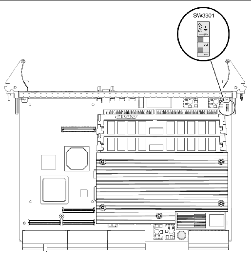

FIGURE B-5 SW3301 DIP Switch Location

Figure showing the location of the SW3301 DIP switch bank.


Note - By default, the SW3301 DIP switches are both set in an open position, which means they are set in the opposite direction of the arrow. FIGURE B-5 shows the two switches in the default, open position.


TABLE B-14 SW3301 Switch Descriptions

Switch

Switch Setting

Description

1

Open

Boot the board from the main OpenBoot PROM image (default setting)


Closed

Boot the board from the backup OpenBoot PROM image in the system flash (see FIGURE 4-2)

2

Open

Board is set to operate in a cPCI server (default setting)


Closed

Board is set to operate in a cPSB chassis


Note - When switch 2 is set to the closed position (the cPSB chassis setting), the board's cPCI bridge will not be taken out of reset.


Note - The Netra CP2500 board is only supported in a Netra CT 410 server, Netra CT 810 server, or a third-party cPSB chassis. Sun does not support operating the Netra CP2500 board in a third-party cPCI server.


1 (TableFootnote) BUSMODE signals require a pull-up.
2 (TableFootnote) Caution - Backplane power (VIO) must be +EP_5V.
3 (TableFootnote) Caution - Select VIO pins must be 5V, and not universal.