| Skip Navigation Links | |
| Exit Print View | |

|
Sun Flash Accelerator F40 PCIe Card User's Guide |
Sun Flash Accelerator F40 PCIe Card Overview
About the Sun Flash Accelerator F40 PCIe Card
Card Software and Firmware Components
Preparing the Card for Installation
Perform ESD Prevention Measures
Update the Host Operating System
Installing the Card Into a Server
Remove an Existing Card From a Server
Servicing the Card Using the ddcli Utility
Show the Vital Product Data Command
Troubleshooting Using Card LEDs
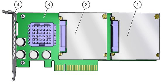
The Sun Flash Accelerator F40 PCIe Card contains these hardware components:
|
The Sun Flash Accelerator F40 PCIe Card is a block storage device, with block sizing optimization capabilities. You can use the card for either nonpersistent or persistent data. The card offers high-performance with low latency and a low CPU burden. The Sun Flash Accelerator F40 PCIe Card is designed with advanced enterprise multi-level cell NAND (eMLC) technology for high-level performance and write durability, while providing higher capacity than SLC NAND cards.
The Sun Flash Accelerator F40 PCIe Card presents itself to the operating system through a Fusion-MPT™ interface as a flash card with four drives, that requires minimal user configuration. The card functions using a SAS controller with drive firmware running on its internal processor. The controller connects to up to four embedded flash memory modules.
For example, one Sun Flash Accelerator F40 PCIe Card displays as follows in an Oracle Solaris operating system:
5. c0t500051610010E810d0 <ATA-3E128-TS2-550B00-T3EM cyl 65533 alt 2 hd 16 sec 186>
/scsi_vhci/disk@g500051610010e810
6. c0t500051610010EA9Cd0 <ATA-3E128-TS2-550B00-T3EM cyl 65533 alt 2 hd 16 sec 186>
 /scsi_vhci/disk@g500051610010ea9c
7. c0t500051610010EC0Cd0 <ATA-3E128-TS2-550B00-T3EM cyl 65533 alt 2 hd 16 sec 186>
 /scsi_vhci/disk@g500051610010ec0c
8. c0t500051610010EC60d0 <ATA-3E128-TS2-550B00-T3EM cyl 65533 alt 2 hd 16 sec 186>
 /scsi_vhci/disk@g500051610010ec60
The Sun Flash Accelerator F40 PCIe Card uses a low-profile, half-height, and half-length PCIe board, as shown in the following illustration.
Figure 1 Sun Flash Accelerator F40 PCIe Card Components

Figure Legend
1 Flash stack 1 (Cage 1)
2 Flash stack 2 (Cage 2)
3 Board
4 Bracket
The card meets the PCI low-profile MD2 specification. The card has a PCIe interface that complies with the PCI Express Specification 2.0.